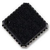
ADP3208CJCPZ-RL ON Semiconductor, ADP3208CJCPZ-RL Datasheet - Page 21

ADP3208CJCPZ-RL
Manufacturer Part Number
ADP3208CJCPZ-RL
Description
IC CTLR BUCK 7BIT IMVP6 48LFCSP
Manufacturer
ON Semiconductor
Datasheet
1.ADP3208CJCPZ-RL.pdf
(37 pages)
Specifications of ADP3208CJCPZ-RL
Applications
Controller, Power Supplies for Next-Generation Intel Processors
Voltage - Input
3.3 ~ 22 V
Number Of Outputs
1
Voltage - Output
0.0125 ~ 1.5 V
Operating Temperature
-10°C ~ 100°C
Mounting Type
Surface Mount
Package / Case
48-LFCSP
Output Voltage
10 mV
Output Current
40 A
Input Voltage
19 V
Supply Current
6 mA
Switching Frequency
300 KHz
Mounting Style
SMD/SMT
Maximum Operating Temperature
+ 100 C
Minimum Operating Temperature
- 10 C
Lead Free Status / RoHS Status
Lead free / RoHS Compliant
Available stocks
Company
Part Number
Manufacturer
Quantity
Price
Company:
Part Number:
ADP3208CJCPZ-RL
Manufacturer:
AD
Quantity:
4 500
Part Number:
ADP3208CJCPZ-RL
Manufacturer:
ON/安森美
Quantity:
20 000
RPM mode. If the load condition is light, the chip enters
Discontinuous Conduction Mode (DCM). Figure 33 shows
a typical single−phase buck with one upper FET, one lower
FET, an output inductor, an output capacitor, and a load
resistor. Figure 34 shows the path of the inductor current
with the upper FET on and the lower FET off. In Figure 35
the high−side FET is off and the low−side FET is on. In
CCM, if one FET is on, its complementary FET must be off;
however, in DCM, both high− and low−side FETs are off and
no current flows into the inductor (see Figure 36). Figure 37
shows the inductor current and switch node voltage in DCM.
switch node voltage to determine when to turn off the
low−side FET. Figure 38 shows a typical waveform in DCM
with a 1 A load current. Between t
ramps down. The current flows through the source drain of
the low−side FET and creates a voltage drop across the FET
with a slightly negative switch node. As the inductor current
ramps down to 0 A, the switch voltage approaches 0 V, as seen
just before t
−6 mV, the low−side FET is turned off.
caused by the LC created from capacitance on the switch
node, including the C
This ringing is normal.
load. Figure 38 shows the typical DCM waveform of the
ADP3208C. As the load increases, the ADP3208C enters
into CCM. In DCM, frequency decreases with load current.
Figure 39 shows switching frequency vs. load current for a
typical design. In DCM, switching frequency is a function
of the inductor, load current, input voltage, and output
voltage.
If DPRSLP is pulled high, the ADP3208C operates in
In DCM with a light load, the ADP3208C monitors the
Figure 37 shows a small, dampened ringing at t
The ADP3208C automatically goes into DCM with a light
Figure 34. Buck Topology Inductor Current During
VOLTAGE
INPUT
2
. When the switch voltage is approximately
Figure 33. Buck Topology
DRVH
DRVL
DS
OFF
of the FETs and the output inductor.
ON
t
Q1
Q2
0
and t
SWITCH
NODE
1
1
and t
L
2
L
, the inductor current
C
C
OUTPUT
VOLTAGE
LOAD
2
LOAD
. This is
http://onsemi.com
21
Figure 37. Inductor Current and Switch Node in DCM
Figure 38. Single−Phase Waveforms in DCM with 1 A
Figure 35. Buck Topology Inductor Current During
Figure 36. Buck Topology Inductor Current During
INDUCTOR
VOLTAGE
CURRENT
SWITCH
NODE
4
2
3
1
t
0
LOW−SIDE GATE DRIVE 5.0 V/DIV
SWITCH NODE 5.0 V/DIV
t
1
OUTPUT VOLTAGE
INDUCTOR CURRENT
20 mV/DIV
5 A/DIV
Load Current
OFF
OFF
OFF
ON
t
t
1
2
and t
and t
t
2 ms/DIV
2
2
3
L
L
t
3
t
4
C
C
LOAD
LOAD


