ISL6263ACRZ Intersil, ISL6263ACRZ Datasheet
ISL6263ACRZ
Specifications of ISL6263ACRZ
Available stocks


Related parts for ISL6263ACRZ


ISL6263ACRZ Summary of contents
Page 1
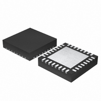
... All other trademarks mentioned are the property of their respective owners. ISL6263A July 8, 2010 FN9284.3 ISL6263A (32 LD 5x5 QFN) TOP VIEW THERMAL PAD (BOTTOM Intersil (and design registered trademark of Intersil Americas Inc. 3 Technology™ trademark of Intersil Americas Inc. VID1 VID0 PVCC LGATE PGND PHASE UGATE BOOT ...
Page 2
... Ordering Information PART NUMBER (Notes 2, 3 ISL6263ACRZ ISL6263 ACRZ ISL6263ACRZ-T (Note 1) ISL6263 ACRZ ISL6263AIRZ ISL6263 AIRZ ISL6263AIRZ-T (Note 1) ISL6263 AIRZ NOTES: 1. Please refer to TB347 for details on reel specifications. 2. These Intersil Pb-free plastic packaged products employ special Pb-free material sets, molding compounds/die attach materials, and 100% matte tin plate plus anneal (e3 termination finish, which is RoHS compliant and compatible with both SnPb and Pb-free soldering operations) ...
Page 3
Block Diagram VDD V REF 1.545V + - VSS 1:1 RBIAS OCSET - OCP VSUM + + DFB - DROOP VO VSEN RTN VDIFF VID0 VID1 VID2 VID DAC DVID VID3 VID4 SOFT FIGURE 1. SIMPLIFIED FUNCTIONAL ...
Page 4
Simplified Application Circuit for DCR Current Sensing C VDD R RBIAS RBIAS C SOFT SOFT PGOOD R PMON PMON C PMON VID<0:4> VR_ON AF_EN FDE V VSEN CC_SNS V RTN SS_SNS FSET FSET C COMP1 COMP R ...
Page 5
Simplified Application Circuit for Resistive Current Sensing C VDD R RBIAS RBIAS C SOFT SOFT PGOOD R PMON PMON C PMON VID<0:4> VR_ON AF_EN FDE V VSEN CC_SNS V RTN SS_SNS FSET FSET C COMP1 COMP R ...
Page 6
... Storage Temperature . . . . . . . . . . . . . . . . . . . . . . . .-65°C to +150°C Pb-free Reflow Profile . . . . . . . . . . . . . . . . . . . . . . . . .see link below http://www.intersil.com/pbfree/Pb-FreeReflow.asp Recommended Operating Conditions Ambient Temp. Range ISL6263ACRZ . . . . . . . . . . . . . . . . . . . . . . . . . . -10°C to +100°C ISL6263AIRZ . . . . . . . . . . . . . . . . . . . . . . . . . . . -40°C to +100°C VIN to VSS +5V to +25V VDD to VSS . . . . . . . . . . . . . . . . . . . . . . . . . . . . . . . . . . . . +5V ±5% PVCC to PGND . . . . . . . . . . . . . . . . . . . . . . . . . . . . . . . . . +5V ±5% FDE to VSS . . . . . . . . . . . . . . . . . . . . . . . . . . . . . . . . . . 0V to +3.3V = -40° ...
Page 7
... Boldface limits apply over the operating temperature range SYMBOL TEST CONDITIONS T = -40°C to +100°C A VID = 0.72100V to 0.51500V T = -40°C to +100°C A VID = 0.41200 T = -40°C to +100° 7kΩ FSET COMP (ISL6263ACRZ 7kΩ FSET COMP (ISL6263AIRZ GBW C = 20pF 20pF 1.28750V FB ...
Page 8
Electrical Specifications These specifications apply for +25° -40°C to +100°C. (Continued) PARAMETER LGATE Source Resistance (Note 7) LGATE Source Current (Note 7) LGATE Sink Resistance (Note 7) LGATE Sink Current (Note 7) UGATE Pull-Down Resistor ...
Page 9
Functional Pin Descriptions RBIAS (Pin 1) - Sets the internal 10µ Connect a 150kΩ ±1% resistor from RBIAS to VSS. SOFT (Pin 2) - Sets the output voltage slew-rate. Connect an X5R or X7R ceramic capacitor from SOFT to VSS. ...
Page 10
... Theory of Operation CORE CCGFX 3 V The R Modulator CCGFX VID0 (V) The heart of the ISL6263A is Intersil’s Robust-Ripple Regulator (R of fixed frequency PWM control, and variable frequency 0 1.28750 hysteretic control that will simultaneously affect the PWM 1 1.26175 switching frequency and PWM duty cycle in response ...
Page 11
VR_ON 90% ~100µ SOFT CCGFX PGOOD 13 SWITCHING CYCLES FIGURE 4. ISL6263A START-UP TIMING Static Regulation The V output voltage will be regulated to the value set CCGFX by the VID inputs per Table 2. A true differential ...
Page 12
OCP + DROOP + − + Σ − VDIFF FIGURE 5. SIMPLIFIED VOLTAGE DROOP CIRCUIT WITH GPU SOCKET KELVIN SENSING AND INDUCTOR DCR CURRENT SENSING Smooth mode transitions are facilitated by the R which correctly maintains ...
Page 13
TABLE 3. FAULT PROTECTION SUMMARY OF ISL6263A FAULT DURATION PRIOR TO PROTECTION FAULT TYPE PROTECTION ACTIONS Overcurrent 120µs LGATE, UGATE, and PGOOD latched low Short Circuit <2µs LGATE, UGATE, and PGOOD latched low Overvoltage 1ms LGATE, UGATE, and (+195mV) PGOOD ...
Page 14
PWM cycle is 200mV. One will find that a bootstrap capacitance of at least 0.125µF is required. The next larger standard value capacitance is 0.15µF. A good quality ceramic capacitor is recommended. ...
Page 15
... FIGURE 8. EQUIVALENT MODEL FOR DROOP CIRCUIT USING INDUCTOR DCR CURRENT SENSING 15 ISL6263A It is recommended to begin your droop design using the NTC evaluation board available from Intersil. (EQ. 9) The gain of the droop amplifier circuit is shown in Equation 15: k droopamp After determining R (EQ. 10) ...
Page 16
OCP + + − FIGURE 9. EQUIVALENT MODEL FOR DROOP CIRCUIT USING DISCRETE RESISTOR CURRENT SENSING The current sensing traces should be routed directly to the inductor pads for accurate DCR voltage drop measurement. However, due to layout imperfection, ...
Page 17
... VID state and the output impedance is 8.0mΩ in order to achieve the 8.0mV/A load line highly recommended to design the compensation such that the regulator output impedance is 8.0mΩ. Intersil provides a spreadsheet to calculate the compensator parameters. Caution needs to be used in choosing the input resistor to the FB pin. Excessively high resistance will cause an error to the output voltage regulation due to the bias current flowing through the FB pin ...
Page 18
... Accordingly, the reader is cautioned to verify that data sheets are current before placing orders. Information furnished by Intersil is believed to be accurate and reliable. However, no responsibility is assumed by Intersil or its subsidiaries for its use; nor for any infringements of patents or other rights of third parties which may result from its use ...
Page 19
Package Outline Drawing L32.5x5 32 LEAD QUAD FLAT NO-LEAD PLASTIC PACKAGE Rev 2, 02/07 5.00 6 PIN 1 INDEX AREA (4X) 0.15 TOP VIEW ( 4. 80 TYP ) ( TYPICAL RECOMMENDED LAND PATTERN 19 ISL6263A A ...