ISL6264CRZ Intersil, ISL6264CRZ Datasheet
ISL6264CRZ
Specifications of ISL6264CRZ
Available stocks


Related parts for ISL6264CRZ

ISL6264CRZ Summary of contents
Page 1
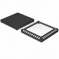
... TEMP (°C) ISL6264CRZ* ISL6264 CRZ -10 to +100 40 Ld 6x6 QFN L40.6x6 ISL6264CRZ-T* ISL6264 CRZ -10 to +100 40 Ld 6x6 QFN *Please refer to TB347 for details on reel specifications. NOTE: These Intersil Pb-free plastic packaged products employ special Pb-free material sets, molding compounds/die attach materials, ...
Page 2
... Thermal Resistance (Typical, Notes 1, 2) θ QFN Package Maximum Junction Temperature . . . . . . . . . . . . . . . . . . . . . . +150°C Maximum Storage Temperature Range . . . . . . . . . .-65°C to +150°C Pb-free reflow profile . . . . . . . . . . . . . . . . . . . . . . . . . .see link below http://www.intersil.com/pbfree/Pb-FreeReflow.asp Recommended Operating Conditions Supply Voltage, VDD . . . . . . . . . . . . . . . . . . . . . . . . . . . . . .+5V ±5% Voltage, VIN +5V to 25V Ambient Temperature . . . . . . . . . . . . . . . . . . . . . . .-10°C to +100°C Junction Temperature . . . . . . . . . . . . . . . . . . . . . . .-10° ...
Page 3
Electrical Specifications VDD = 5V, T tested at +25°C, unless otherwise specified. Temperature limits established by characterization and are not production tested. (Continued) SYMBOL PARAMETER ISEN1, ISEN2 Imbalance Voltage Input Bias Current SOFT START CURRENT I Soft Start Current SS ...
Page 4
Electrical Specifications VDD = 5V, T tested at +25°C, unless otherwise specified. Temperature limits established by characterization and are not production tested. (Continued) SYMBOL PARAMETER OFFSET FUNCTION I OFS Pin Current OFFSET I FB Pin Souring Current FB LOGIC INPUTS ...
Page 5
Functional Pin Description SET 1 RBIAS 2 OFS 3 SOFT 4 OCSET 5 GND PAD (BOTTOM COMP VDIFF 9 VSEN ...
Page 6
PVCC 5V power supply for gate drivers. LGATE1 Lower-side MOSFET gate signal for phase 1. PGND1 The return path of the lower gate driver for phase 1. PHASE1 The phase node of phase 1. This pin should connect to the ...
Page 7
Function Block Diagram RBIAS VID0 VID1 VID2 DAC VID3 DACOUT VID4 VID5 MODE CHANGE REQUEST VR_ON MODE PSI_L CONTROL 0.5 10uA OCSET VO - DROOP DFB + DROOP - VSEN RTN PGOOD VO PGOOD ...
Page 8
Simplified Application Circuit for DCR Current Sensing VID<0:5> R OFS PSI_L SET VR_ON CPU_PWRGD REMOTE SENSE FSET C 9 FIGURE 2. ISL6264 BASED ...
Page 9
Simplified Application Circuit for Resistor Current Sensing VID<0:5> R OFS PSI_L SET VR_ON CPU_PWRGD REMOTE SENSE FSET C 9 FIGURE 3. ISL6264 BASED ...
Page 10
Typical Performance Curves 100 90 80 VIN = 8.0V VIN = 12.6V 70 VIN = 19. (A) OUT FIGURE 4. ACTIVE MODE EFFICIENCY, 2 PHASE, CCM, PSI_l ...
Page 11
Typical Performance Curves VR_ON VR_ON FIGURE 10. SOFT START WAVEFORM AT VID = 1.55V, ILOAD = FIGURE 12. SOFT START WAVEFORM SHOWING CURRENT SHARING AT VIN = 12.6V, VID = 1.2V AND ILOAD ...
Page 12
Typical Performance Curves Phase1 PHASE1 FIGURE 16. LOAD APPLICATION RESPONSE AT 2-PHASE CCM, VIN = 19V, ILOAD = 10A→46A, AND VID = 1.15V Phase1 PHASE1 FIGURE 18. LOAD APPLICATION RESPONSE AT 1-PHASE DE MODE, ...
Page 13
Typical Performance Curves Ugate UGATE FIGURE 22. GATE DRIVER WAVEFORMS AT VIN = 8V, ILOAD = 40A IRF7821 AS UPPER MOSFET AND 2 X IRF7832 AS LOWER MOSFET Phase1 PHASE1 FIGURE 24. DEEPER SLEEP MODE ...
Page 14
... DCM-mode operation when PSI_L is asserted to logic low. 3 The heart of the ISL6264 is the R Technology™, Intersil's Robust Ripple Regulator modulator. The R combines the best features of fixed frequency PWM and hysteretic PWM while eliminating many of their shortcomings. The ISL6264 modulator internally synthesizes ...
Page 15
TABLE 1. V TABLE FOR AMD 6-BIT V ID VID5 VID4 VID3 VID2 VID1 ...
Page 16
... SOFT 1-DE (diode emulation) capacitor. The internal current source of 230µA is used to charge or discharge the SOFT capacitor. Intersil result, high-speed input voltage steps do not result in significant output voltage perturbations. In response to load current step increases, the ISL6264 will transiently raise the switching frequency so that response time is decreased and current is shared by two channels ...
Page 17
Undervoltage protection is independent of the overcurrent limit. If the output voltage is less than the VID set value by 300mV or more, a fault will latch after one millisecond in that condition. The PWM outputs will turn off and ...
Page 18
Using a SLEWRATE of 4.2mV/µs, and the typical I given in the Electrical Specification table of 230µA, C shown in Equation 3: ≡ ⁄ 230μA 4.2 SOFT A choice of 0.047µF would guarantee a SLEWRATE ...
Page 19
OC + DROOP INTERNAL TO ISL6264 + RTN VD IFF FIGURE 32. SIMPLIFIED SCHEMATIC FOR DROOP AND DIE SENSING WITH INDUCTOR DCR CURRENT SENSING Setting the Switching Frequency - FSET ...
Page 20
... R drp2 is provided by Intersil. Do not let the mismatch get larger than 600Ω. To reduce the mismatch, multiply both R factor. The appropriate factor in the example is 1404/853 = 1.65. In summary, the predicted load line with (EQ ...
Page 21
INDUCTOR TEMPERATURE (°C) FIGURE 33. LOAD LINE PERFORMANCE WITH NTC THERMAL COMPENSATION Dynamic Mode of Operation - Dynamic Droop Using DCR Sensing Droop is very important for load transient performance. If ...
Page 22
... Accordingly, the reader is cautioned to verify that data sheets are current before placing orders. Information furnished by Intersil is believed to be accurate and reliable. However, no responsibility is assumed by Intersil or its subsidiaries for its use; nor for any infringements of patents or other rights of third parties which may result from its use ...
Page 23
Package Outline Drawing L40.6x6 40 LEAD QUAD FLAT NO-LEAD PLASTIC PACKAGE Rev 3, 10/06 6.00 6 PIN 1 INDEX AREA 0.15 (4X) TOP VIEW ( TYP ) ( TYPICAL RECOMMENDED LAND PATTERN 23 ...