ISL6265AHRTZ Intersil, ISL6265AHRTZ Datasheet
ISL6265AHRTZ
Specifications of ISL6265AHRTZ
Available stocks


Related parts for ISL6265AHRTZ

ISL6265AHRTZ Summary of contents
Page 1
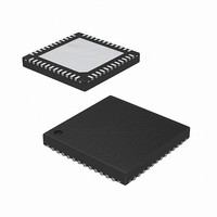
... ISL6265AHRTZ 6265A HRTZ -10 to +100 48 Ld 6x6 TQFN L48.6x6 ISL6265AHRTZ-T* 6265A HRTZ -10 to +100 48 Ld 6x6 TQFN *Please refer to TB347 for details on reel specifications. NOTE: These Intersil Pb-free plastic packaged products employ special Pb-free material sets, molding compounds/die attach materials, ...
Page 2
Function Block Diagram RTN_NB SVC NO DROOP SVD PSI_L I_OFS PWROK VREF_NB VREF0 VREF1 OFS/FIXEN OCSET_NB OCSET RBIAS VW0 COMP0 FB0 VDIFF0 V0 VSEN0 1 RTN0 DROOP ISP0 CURRENT SENSE ISN0 ISP1 CURRENT SENSE ISN1 V1 VSEN1 1 RTN1 VDIFF1 ...
Page 3
Simplified Application Circuit for Dual Plane and Northbridge Support SVI DATA SVI CLOCK ENABLE PWROK VDDPWRGD REMOTE SENSE REMOTE SENSE VDD_PLANE_STRAP FIGURE 2. ISL6265A BASED DUAL-PLANE AND NORTHBRIDGE CONVERTERS WITH INDUCTOR DCR CURRENT SENSING 3 ISL6265A VIN +5V VIN VCC ...
Page 4
Simplified Application Circuit for Uniplane Core and Northbridge Support SVI DATA SVD SVI CLOCK SVC ENABLE EN PWROK PWROK VDDPWRGD PGOOD VSEN0 REMOTE SENSE RTN0 REMOTE VSEN1 SENSE VDD_PLANE_STRAP RTN1 OFS/VFIXEN VDIFF0 FB0 COMP0 VW0 VDIFF1 OPEN OPEN FB1 COMP1 ...
Page 5
Simplified Application Circuit for Dual Layout +5V SVI DATA SVD SVI CLOCK SVC ENABLE EN PWROK PWROK VDDPWRGD PGOOD VSEN0 REMOTE SENSE RTN0 VDD_PLANE_STRAP +1.8V RTN1 REMOTE DNP UNIPLANE SENSE VSEN1 OFS/VFIXEN VDIFF0 FB0 COMP0 VW0 VDIFF1 FB1 COMP1 VW1 ...
Page 6
... Thermal Resistance (Typical, Notes 1, 2) θ TQFN . . . . . . . . . . . . . . . . . . . . Maximum Junction Temperature . . . . . . . . . . . . . . . . . . . . . . +150°C Maximum Storage Temperature Range . . . . . . . . . .-65°C to +150°C Pb-Free Reflow Profile .see link below http://www.intersil.com/pbfree/Pb-FreeReflow.asp Recommended Operating Conditions Supply Voltage, VCC, PVCC . . . . . . . . . . . . . . . . . . . . . . . .+5V ±5% Battery Voltage, VIN . . . . . . . . . . . . . . . . . . . . . . . . . . . . +6V to 24V Ambient Temperature . . . . . . . . . . . . . . . . . . . . . . .-10°C to +100°C Junction Temperature . . . . . . . . . . . . . . . . . . . . . . .-10° ...
Page 7
Electrical Specifications VCC = PVCC = 5V, V MAX limits are 100% tested at +25°C, unless otherwise specified. Temperature limits established by characterization and are not production tested (Continued) PARAMETER SYMBOL CORE CURRENT SENSE Current Imbalance Threshold Input Bias Current ...
Page 8
Electrical Specifications VCC = PVCC = 5V, V MAX limits are 100% tested at +25°C, unless otherwise specified. Temperature limits established by characterization and are not production tested (Continued) PARAMETER SYMBOL OFFSET FUNCTION OFS Pin Voltage For Droop Enabling FB ...
Page 9
Functional Pin Description OFS/VFIXEN 2 PGOOD 3 PWROK 4 SVD 5 SVC 6 49 ENABLE GND 7 RBIAS [BOTTOM] 8 OCSET 9 VDIFF0 10 FB0 11 COMP0 12 VW0 ...
Page 10
... PWM pulse widths. Operating on these large-amplitude, noise-free synthesized signals allows the ISL6265A to achieve lower output ripple and lower phase jitter than either conventional hysteretic or fixed frequency PWM controllers. Unlike conventional hysteretic converters, the ISL6265A has 3 Technology™, Intersil's 3 modulator FN6884.0 May 11, 2009 ...
Page 11
... Modulator The ISL6265A modulator features Intersil’s R hybrid of fixed frequency PWM control and variable frequency hysteretic control (see Figure 5). Intersil’s R simultaneously affect the PWM switching frequency and PWM duty cycle in response to input voltage and output load 3 transients ...
Page 12
CPU Core1 negative sense and connect the RTN1 pin to a pull-up resistor. Mode Selection The OFS/VFIXEN pin selects between the AMD defined VFIX and SVI modes of operation and enables droop if desired in SVI mode only. ...
Page 13
At the end of the soft-start interval, the PGOOD output transitions high indicating all output planes are within regulation limits. If the EN input falls below the enable falling threshold, the ...
Page 14
VOLTAGE SVID[6:0] (V) SVID[6:0] 000_0000b 1.5500 010_0000b 000_0001b 1.5375 010_0001b 000_0010b 1.5250 010_0010b 000_0011b 1.5125 010_0011b 000_0100b 1.5000 010_0100b 000_0101b 1.4875 010_0101b 000_0110b 1.4750 010_0110b 000_0111b 1.4625 010_0111b 000_1000b 1.4500 010_1000b 000_1001b 1.4375 010_1001b 000_1010b 1.4250 010_1010b 000_1011b 1.4125 010_1011b ...
Page 15
SVC SVD SLAVE ADDRESS PHASE SVI Bus Protocol The AMD processor bus protocol is compliant with SMBus send byte protocol for VID transactions (see Figure 8). During a send byte transaction, the processor sends the start sequence ...
Page 16
It is recommended that whenever the control loop compensation network is modified, the switching frequency should be checked and adjusted by changing R necessary. Current Sense Core and Northbridge regulators feature two different types of current sense circuits. CORE CONTINUOUS ...
Page 17
NORTHBRIDGE CURRENT SENSE During the off-time following a PHASE transition low, the Northbridge controller samples the voltage across the lower MOSFET ground-referenced amplifier is DS(ON) connected to the PHASE node through a resistor The voltage ...
Page 18
Efficiency can be further improved with a reduction of unnecessary switching losses by reducing the PWM 3 frequency characteristic of the R PWM frequency to decrease while in diode emulation. The extent of the frequency reduction is proportional ...
Page 19
... This design guide is intended to provide a high-level explanation of the steps necessary to design a single-phase power converter assumed that the reader is familiar with many of the basic skills and techniques referenced in the following section. In addition to this guide, Intersil provides complete reference designs that include schematics, bills of sensing DS(ON) materials, and example board layouts ...
Page 20
The output capacitors must supply or sink load current while the current in the output inductors increases or decreases to meet the demand. The duty cycle of ...
Page 21
I = 0.75 0.1 P-P,N I P-P 0.2 0.4 DUTY CYCLE (V FIGURE 12. NORMALIZED RMS INPUT CURRENT FOR 2-PHASE CONVERTER MOSFET Selection and Considerations The choice of MOSFETs depends on the current each MOSFET will ...
Page 22
... Accordingly, the reader is cautioned to verify that data sheets are current before placing orders. Information furnished by Intersil is believed to be accurate and reliable. However, no responsibility is assumed by Intersil or its subsidiaries for its use; nor for any infringements of patents or other rights of third parties which may result from its use ...
Page 23
Package Outline Drawing L48.6x6 48 LEAD THIN QUAD FLAT NO-LEAD PLASTIC PACKAGE Rev 1, 4/07 6.00 6 PIN 1 INDEX AREA (4X) 0.15 TOP VIEW ( 5. 75 TYP ) ( TYPICAL RECOMMENDED LAND PATTERN 23 ISL6265A ...