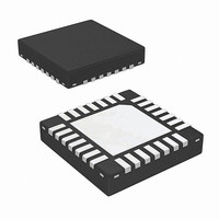
ISL62881CHRTZ Intersil, ISL62881CHRTZ Datasheet - Page 3

ISL62881CHRTZ
Manufacturer Part Number
ISL62881CHRTZ
Description
IC REG PWM SGL PHASE 28TQFN
Manufacturer
Intersil
Datasheet
1.ISL62881CHRTZ.pdf
(37 pages)
Specifications of ISL62881CHRTZ
Applications
Controller, Intel IMVP-6.5™
Voltage - Input
4.5 ~ 25 V
Number Of Outputs
1
Voltage - Output
0.0125 ~ 1.5 V
Operating Temperature
-10°C ~ 100°C
Mounting Type
Surface Mount
Package / Case
28-VQFN
For Use With
ISL62881CCPUEVAL2Z - EVAL BOARD ISL62881CCPU 28QFN
Lead Free Status / RoHS Status
Lead free / RoHS Compliant
Available stocks
Company
Part Number
Manufacturer
Quantity
Price
Part Number:
ISL62881CHRTZ
Manufacturer:
INTERSIL
Quantity:
20 000
Part Number:
ISL62881CHRTZ-T
Manufacturer:
INTERSIL
Quantity:
20 000
Pin Function Description
ISL62881C ISL62881D
20, 21, 22,
23, 24, 25,
9, 10
pad
11
12
13
14
15
16
17
18
19
26
27
28
4
5
6
7
8
-
-
23, 24, 25,
26, 27, 28
11, 12
10
13
14
15
16
17
18
19
20
21
22
29
30
31
6
7
8
9
-
VID5, VID6
3
ISUM- and
DPRSLPVR
SYMBOL
BOTTOM
LGATEa
LGATEb
ISUM+
VR_ON
UGATE
PHASE
LGATE
COMP
VSEN
IMON
BOOT
VID0,
VID1,
VID2,
VID3,
VID4,
VSSP
VCCP
VDD
RTN
VIN
VW
FB
A resistor from this pin to COMP programs the switching frequency (8kΩ gives
approximately 300kHz).
This pin is the output of the error amplifier. Also, a resistor across this pin and GND
adjusts the overcurrent threshold.
This pin is the inverting input of the error amplifier.
Remote core voltage sense input. Connect to microprocessor die.
Remote voltage sensing return. Connect to ground at microprocessor die.
Droop current sense input.
5V bias power.
Power stage supply voltage, used for feed-forward.
An analog output. IMON outputs a current proportional to the regulator output
current.
Connect an MLCC capacitor across the BOOT and the PHASE pin. The boot capacitor
is charged through an internal boot diode connected from the VCCP pin to the BOOT
pin, each time the PHASE pin drops below VCCP minus the voltage dropped across the
internal boot diode.
Output of the high-side MOSFET gate driver. Connect the UGATE pin to the gate of the
high-side MOSFET.
Current return path for the high-side MOSFET gate driver. Connect the PHASE pin to
the node consisting of the high-side MOSFET source, the low-side MOSFET drain, and
the output inductor.
Current return path for the low-side MOSFET gate driver. Connect the VSSP pin to the
source of the low-side MOSFET through a low impedance path, preferably in parallel
with the traces connecting the LGATE pins to the gates of the low-side MOSFET.
Output of the low-side MOSFET gate driver. Connect the LGATE1 pin to the gate of the
Phase-1 low-side MOSFET.
Output of the low-side MOSFET gate driver that is always active. Connect the LGATEa
pin to the gate of the low-side MOSFET that is active all the time.
Another output of the low-side MOSFET gate driver. This gate driver will be pulled low
when the DPRSLPVR pin logic is high. Connect the LGATEb pin to the gate of the
low-side MOSFET that is idle in deeper sleep mode.
Input voltage bias for the internal gate drivers. Connect +5V to the VCCP pin.
Decouple with at least 1µF of an MLCC capacitor to the VSSP pin.
VID input with VID0 = LSB and VID6 = MSB.
Voltage regulator enable input. A high level logic signal on this pin enables the
regulator.
Deeper sleep enable signal. A high level logic signal on this pin indicates that the
microprocessor is in deeper sleep mode.
The bottom pad is electrically connected to the GND pin inside the IC. It should also
be used as the thermal pad for heat removal.
ISL62881C, ISL62881D
ISL62881C, ISL62881D
(Continued)
DESCRIPTION
March 8, 2010
FN7596.0


