ISL6227IAZ Intersil, ISL6227IAZ Datasheet
ISL6227IAZ
Specifications of ISL6227IAZ


Related parts for ISL6227IAZ

ISL6227IAZ Summary of contents
Page 1
... NUMBER MARKING ISL6227CA* ISL 6227CA ISL6227CAZ* ISL 6227CAZ -10 to +100 28 Ld QSOP (Note) ISL6227IA* ISL 6227IA ISL6227IAZ* ISL 6227IAZ (Note) ISL6227HRZ* ISL 6227HRZ -10 to +100 28 Ld QFN (Note) ISL6227IRZ* ISL 6227IRZ (Note) *Add “-T” suffix for tape and reel. Please refer to TB347 for details on reel specifications ...
Page 2
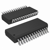
Pinouts ISL6227 28 LD QSOP TOP VIEW 1 GND 2 LGATE1 PGND1 3 4 PHASE1 5 UGATE1 BOOT1 6 7 ISEN1 EN1 8 VOUT1 9 VSEN1 10 OCSET1 11 SOFT1 12 DDR 13 VIN 14 Generic Application Circuits V IN ...
Page 3
... Thermal Resistance (Typical) QSOP Package (Note 2) QFN Package (Notes 3, 4) Maximum Junction Temperature (Plastic Package +150°C Maximum Storage Temperature Range . . . . . . . . . .-65°C to +150°C + 0.3V Pb-Free Reflow Profile .see link below CC http://www.intersil.com/pbfree/Pb-FreeReflow.asp ± 5% SYMBOL TEST CONDITIONS I LGATEx, UGATEx Open, VSENx forced above CC regulation point, V > ...
Page 4
Electrical Specifications Recommended Operating Conditions, Unless Otherwise Noted. Parameters with MIN and/or MAX limits are 100% tested at +25°C, unless otherwise specified. Temperature limits established by characterization and are not production tested. (Continued) PARAMETER Soft-Start Current During Start-Up Soft-Start Complete ...
Page 5
Typical Operation Performance 100 EFF@ 5V EFF@ 12V EFF@ 5V, PWM 60 EFF@ 12V, PWM EFF@ 19.5V, PWM 0.01 0.10 LOAD CURRENT (A) FIGURE 1. EFFICIENCY OF CHANNEL 1, 2.5V, HYS/PWM ...
Page 6
Typical Operation Performance Vo1 VO1 VPHASE1 Vphase1 ILO1 Ilo1 VO2 Vo2 FIGURE 7. LOAD TRANSIENT ( CHANNEL 1) (DIODE EMULATION MODE) Vo1 VO1 VPHASE2 Vphase2 ILO2 Ilo2 VO2 Vo2 FIGURE 9. LOAD TRANSIENT ( ...
Page 7
Typical Operation Performance Vin1 VIN1 Vo1 VO1 VO2 Vo2 FIGURE 13. INPUT STEP-DOWN TRANSIENT AT PWM MODE EN1 EN1 PG1 PG1 SOFT1 SOFT1 Vo1 VO1 FIGURE 15. SOFT-START INTERVAL AT ZERO INITIAL VOLTAGE OF VO VO1 Vo1 Vphase1 VPHASE1 ILO1 ...
Page 8
Typical Operation Performance VO1 Vo1 PG1 PG1 ILO1 Ilo1 VO2 Vo2 FIGURE 19. OVERCURRENT PROTECTION AT CHANNEL 1 VO1 Vo1 VPHASE1 Vphase1 ILO1 Ilo1 VO2 Vo2 FIGURE 21. MODE TRANSITION OF HYS EN1 EN1 PG1 PG1 SOFT1 SOFT1 Vo1 VO1 ...
Page 9
Typical Operation Performance VDDQ VDDQ PGOOD1 PGOOD1 VTT VTT IL1 IL1 FIGURE 25. VIN = 19V, VDDQ 3A STEP LOAD, VTT 0A LOAD VDDQ VDDQ VTT VTT OCSET2 OCSET2 IL2 IL2 FIGURE 27. VIN = 19V, LOAD STEP ON VTT, ...
Page 10
Functional Pin Description GND Signal ground for the IC. LGATE1, LGATE2 These are the outputs of the lower MOSFET drivers. PGND1, PGND2 These pins provide the return connection for lower gate drivers, and are connected to sources of the lower ...
Page 11
PG2/REF This pin has a double function, depending on the mode of operation. When the chip is used as a dual channel PWM controller (DDR = 0), the pin provides an open drain PGOOD2 function for the second channel the ...
Page 12
BAT54W Cin1 Cin1 Cbt1 Cb 0.15µ µ Lo1 V1 (2.5V 4.7µH Rfb11 17.8k Co11 Co12 220 F 220 F µ 4.7 F µ Cfb1 0.01 F µ FDS6912A FDS6912A Rfb12 Rfb12 ...
Page 13
Block Diagram BOOT1 UGATE1 PHASE1 ADAPTIVE DEAD-TIME DIODE EMULATION PGND1 V/I SAMPLE TIMING PWM/HYS TRANSITION LGATE1 VCC MODE CHANGE COMP 1 SAME STATE FOR 8 CLOCK CYCLES REQUIRED TO CHANGE PWM OR HYS MODE HYSTERETIC COMPARATOR 1 ΔV = 15mV ...
Page 14
Theory of Operation Operation The ISL6227 is a dual channel PWM controller intended for use in power supplies for graphic chipsets, SDRAM, DDR DRAM, or other low voltage power applications in modern notebook and sub-notebook PCs. The IC integrates two ...
Page 15
Output Voltage Program The output voltage of either channel is set by a resistive divider from the output to ground. The center point of the divider is connected to the VSEN pin as shown in Figure 34. The output voltage ...
Page 16
VOUT IIND PHASE COMP MODE PWM OF OPERA T ION FIGURE 35. CCM—HYSTERETIC TRANSITION VOUT IIND PHASE COMP HYSTERETIC MODE OF OPERA T ION FIGURE 36. HYSTERETIC—CCM ...
Page 17
PWM comparator input. This effectively creates an internal current control loop. The resistor connected to the ISEN pin sets the gain in the current sensing. The following expression estimates the required value of the current sense ...
Page 18
TO PWM COMPARATOR - + 0.9V Vc 4.4k ISEN FIGURE 38. THE INTERNAL COMPENSATOR Its transfer function can be written as Equation 12: ⎛ ⎞ ⎛ • 1.857 10 -------------- - 1 -------------- - ...
Page 19
Voltage Monitor and Protections The converter output is monitored and protected against extreme overload, short circuit, overvoltage, and undervoltage conditions. A sustained overload on the output sets the PGOOD low and latches off the offending channel of the chip. The ...
Page 20
OVP comparator is disengaged. The MOSFET driver will restore its normal operation. When the OVP occurs, the PGOOD will drop to low as well. This OVP scheme provides a ‘soft’ crowbar function, which helps clamp the voltage overshoot, ...
Page 21
Application Information Design Procedures GENERAL A ceramic decoupling capacitor should be used between the VCC and GND pin of the chip. There are three major currents drawn from the decoupling capacitor: 1. the quiescent current, supporting the internal logic and ...
Page 22
Based on the above description and functional block diagram, the OC set resistor can be calculated as Equation 18: 10.3V --------------------------------------------------- R = set -------------------------------- - 8μ 140 + CS I ...
Page 23
MOSFET and the source terminal of the lower MOSFET, in order to clamp the parasitic voltage ringing at the phase node in switching. Choosing MOSFETs For a notebook battery with a maximum voltage of 28V, at least a minimum 30V ...
Page 24
Tuning the Turn-on of Upper MOSFET The turn-on speed of the upper MOSFET can be adjusted by the resistor connecting the boot cap to the BOOT pin of the chip. This resistor can confine the voltage ringing on the boot ...
Page 25
PHASE1 and PHASE2 These traces should be short, and positioned away from other weak signal traces. The phase node has a very high dv/dt with a voltage swing from the input voltage to ground. No trace should be in parallel ...
Page 26
Package Outline Drawing L28.5x5 28 LEAD QUAD FLAT NO-LEAD PLASTIC PACKAGE Rev 2, 10/07 5.00 6 PIN 1 INDEX AREA (4X) 0.15 TOP VIEW ( 4. 65 TYP ) ( 3. 10) TYPICAL RECOMMENDED LAND PATTERN 26 ISL6227 A B ...
Page 27
... Accordingly, the reader is cautioned to verify that data sheets are current before placing orders. Information furnished by Intersil is believed to be accurate and reliable. However, no responsibility is assumed by Intersil or its subsidiaries for its use; nor for any infringements of patents or other rights of third parties which may result from its use ...