ISL6334DCRZ Intersil, ISL6334DCRZ Datasheet - Page 23
ISL6334DCRZ
Manufacturer Part Number
ISL6334DCRZ
Description
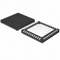
IC CTRLR PWM 4PHASE VR11.1 40QFN
Manufacturer
Intersil
Datasheet
1.ISL6334DCRZ-T.pdf
(28 pages)
Specifications of ISL6334DCRZ
Applications
Controller, Intel VR11.1
Voltage - Input
3 ~ 12 V
Number Of Outputs
1
Voltage - Output
0.5 ~ 1.6 V
Operating Temperature
0°C ~ 70°C
Mounting Type
Surface Mount
Package / Case
40-VFQFN, 40-VFQFPN
Lead Free Status / RoHS Status
Lead free / RoHS Compliant
Available stocks
Company
Part Number
Manufacturer
Quantity
Price

Part Number:
ISL6334DCRZ-T
Manufacturer:
INTERSIL
Quantity:
20 000


MOSFETs
The choice of MOSFETs depends on the current each
MOSFET will be required to conduct; the switching
frequency; the capability of the MOSFETs to dissipate heat;
and the availability and nature of heat sinking and air flow.
LOWER MOSFET POWER CALCULATION
The calculation for heat dissipated in the lower MOSFET is
simple, since virtually all of the heat loss in the lower
MOSFET is due to current conducted through the channel
resistance (r
continuous output current; I
current (see Equation 1); d is the duty cycle (V
L is the per-channel inductance.
An additional term can be added to the lower-MOSFET loss
equation to account for additional loss accrued during the
dead time when inductor current is flowing through the
lower-MOSFET body diode. This term is dependent on the
diode forward voltage at I
frequency, F
the beginning and the end of the lower-MOSFET conduction
interval respectively.
Thus the total maximum power dissipated in each lower
MOSFET is approximated by the summation of P
P
UPPER MOSFET POWER CALCULATION
In addition to r
MOSFET losses are due to currents conducted across the
input voltage (V
higher portion of the upper MOSFET losses are dependent on
switching frequency, the power calculation is more complex.
Upper MOSFET losses can be divided into separate
components involving the upper MOSFET switching times;
the lower MOSFET body-diode reverse-recovery charge, Q
and the upper MOSFET r
When the upper MOSFET turns off, the lower MOSFET does
not conduct any portion of the inductor current until the
voltage at the phase node falls below ground. Once the
lower MOSFET begins conducting, the current in the upper
MOSFET falls to zero as the current in the lower MOSFET
ramps up to assume the full inductor current. In Equation 23,
the required time for this commutation is t
approximated associated power loss is P
P
P
P
LOW,2
LOW 1
LOW 2
UP 1 ,
,
,
≈
.
V
=
=
IN
r
V
⎛
⎝
DS ON
DS(ON)
sw
D ON
I
----- -
N
M
(
DS(ON)
(
; and the length of dead times, t
+
IN
I
--------- -
)
) during switching. Since a substantially
P-P
2
)
F
). In Equation 21, I
⎛
⎜
⎝
sw
⎞ t
⎠
I
----- -
N
M
losses, a large portion of the upper
⎛
⎜
⎝
⎞
⎟
⎠
----
2
⎛
⎝
1
2
I
----- -
N
⎞
⎟
⎠
M
DS(ON)
(
M
1 d
f
S
+
, V
P-P
–
I
--------- -
23
P-P
D(ON)
2
)
is the peak-to-peak inductor
+
⎞ t
⎠
conduction loss.
I
----------------------------------- -
L P-P
d1
(
; the switching
+
12
M
)
2
⎛
⎜
⎝
(
I
----- -
is the maximum
N
M
1 d
UP,1
1
–
–
and the
I
--------- -
P-P
.
)
2
OUT
d1
⎞
⎟
⎠
LOW,1
and t
t
/V
d2
IN
(EQ. 21)
(EQ. 22)
(EQ. 23)
); and
d2
and
, at
rr
ISL6334D
;
At turn-on, the upper MOSFET begins to conduct and this
transition occurs over a time t
approximate power loss is P
A third component involves the lower MOSFET’s reverse
recovery charge, Q
commutated to the upper MOSFET before the lower
MOSFET’s body diode can draw all of Q
through the upper MOSFET across V
dissipated as a result is P
Equation 25:
Finally, the resistive part of the upper MOSFET’s is given in
Equation 26 as P
The total power dissipated by the upper MOSFET at full load
can now be approximated as the summation of the results
from Equations 23, 24, and 25. Since the power equations
depend on MOSFET parameters, choosing the correct
MOSFETs can be an iterative process involving repetitive
solutions to the loss equations for different MOSFETs and
different switching frequencies, as shown in Equation 26.
Current Sensing Resistor
The resistors connected to the ISEN+ pins determine the
gain in the channel-current balance loop and set the
overcurrent trip point. Select values for these resistors by
using Equation 27:
where R
pin, N is the active channel number, R
the current sense element, either the DCR of the inductor or
R
desired overcurrent trip point. Typically, I
to be 1.2x the maximum load current of the specific
application.
With integrated temperature compensation, the sensed
current signal is independent on the operational temperature
of the power stage, i.e. the temperature effect on the current
sense element R
temperature compensation function. R
should be the resistance of the current sense element at the
room temperature.
When the integrated temperature compensation function is
disabled by pulling the TCOMP pin to GND, the sensed
current will be dependent on the operational temperature of
P
P
P
R
UP 2 ,
UP 3 ,
UP 4 ,
SENSE
ISEN
≈
≈
=
=
r
V
DS ON
ISEN
V
depending on the sensing method, and I
IN
-------------------------- -
105 10
IN
(
⎛
⎜
⎝
Q
I
----- -
R
N
M
×
is the sense resistor connected to the ISEN+
rr
X
)
–
f
⎛
⎜
⎝
S
–
I
--------- -
X
UP,4
P-P
I
----- -
6
N
2
M
is cancelled by the integrated
rr
⎞
⎟
⎠
I
------------- -
OCP
⎞ t
⎟
⎠
. Since the inductor current has fully
2
N
⎛
⎜
⎝
.
d
----
2
2
+
⎞
⎟
⎠
I
--------- - d
UP,3
P-P
12
f
S
UP,2
2
2
and is approximated in
. In Equation 24, the
.
IN
X
X
. The power
is the resistance of
rr
OCP
in Equation 27
, it is conducted
can be chosen
August 31, 2010
OCP
(EQ. 26)
(EQ. 24)
(EQ. 25)
(EQ. 27)
FN6802.2
is the
Related parts for ISL6334DCRZ
Image
Part Number
Description
Manufacturer
Datasheet
Request
R

Part Number:
Description:
VR11.1, 4-Phase PWM Controller with Light Load Efficiency Enhancement and Load Current Monitoring
Manufacturer:
INTERSIL [Intersil Corporation]
Datasheet:

Part Number:
Description:
Intersil Corporation [CMOS Serial Controller Interface]
Manufacturer:
Intersil Corporation
Datasheet:
Part Number:
Description:
Manufacturer:
Intersil Corporation
Datasheet:
Part Number:
Description:
357-036-542-201 CARDEDGE 36POS DL .156 BLK LOPRO
Manufacturer:
Intersil Corporation
Datasheet:
Part Number:
Description:
1024-Word x 4-Bit LSI Static RAM
Manufacturer:
Intersil Corporation
Datasheet:
Part Number:
Description:
General Purpose NPN Transistor Arrays FN341.4
Manufacturer:
Intersil Corporation
Datasheet:
Part Number:
Description:
CMOS 16-Bit Microprocessor
Manufacturer:
Intersil Corporation
Datasheet:
Part Number:
Description:
Manufacturer:
Intersil Corporation
Datasheet:
Part Number:
Description:
Manufacturer:
Intersil Corporation
Datasheet:
Part Number:
Description:
Manufacturer:
Intersil Corporation
Datasheet:
Part Number:
Description:
Manufacturer:
Intersil Corporation
Datasheet:
Part Number:
Description:
CMOS 6-Bit Latch and Decoder Memory Interfaces
Manufacturer:
Intersil Corporation
Datasheet:
Part Number:
Description:
CA3046General Purpose NPN Transistor Arrays
Manufacturer:
Intersil Corporation
Datasheet:
Part Number:
Description:
Manufacturer:
Intersil Corporation
Datasheet:
Part Number:
Description:
TR909 DLC/FLC SLIC with Low Power Standby
Manufacturer:
Intersil Corporation
Datasheet: