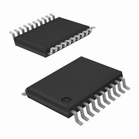
EL7583IREZ-T13 Intersil, EL7583IREZ-T13 Datasheet - Page 13

EL7583IREZ-T13
Manufacturer Part Number
EL7583IREZ-T13
Description
IC CONV DC/DC 3CHN 20-HTSSOP
Manufacturer
Intersil
Datasheet
1.EL7583IR.pdf
(16 pages)
Specifications of EL7583IREZ-T13
Applications
Converter, TFT, LCD
Voltage - Input
2.7 ~ 14 V
Number Of Outputs
2
Voltage - Output
5 ~ 17 V
Operating Temperature
-40°C ~ 85°C
Mounting Type
Surface Mount
Package / Case
20-TSSOP Exposed Pad, 20-eTSSOP, 20-HTSSOP
Lead Free Status / RoHS Status
Lead free / RoHS Compliant
Available stocks
Company
Part Number
Manufacturer
Quantity
Price
Company:
Part Number:
EL7583IREZ-T13
Manufacturer:
INTERSIL
Quantity:
3 100
Two-Stage Negative Charge Pump Circuit
The maximum V
R
where V
Over-Temperature Protection
An internal temperature sensor continuously monitors the
die temperature. In the event that die temperature exceeds
the thermal trip point, the device will shut down and disable
itself. The upper and lower trip points are typically set to
130°C and 90°C respectively.
PCB Layout Guidelines
Careful layout is critical in the successful operation of the
application. The following layout guidelines are
recommended to achieve optimum performance.
• V
• Place the boost converter diode and inductor close to the
• Place the boost converter output capacitor close to the
• Locate feedback dividers close to their respected
• Switching output PCB traces should not cross, or be laid
V
V
V
21
OFF
OFF
DDN
to the pins.
LX pins.
PGND pins.
feedback pins to avoid switching noise coupling into the
high impedance node.
out adjacent to, feedback traces without using a grounded
REF
and R
(
max
=
- N
REF
and V
-V
×
22
)
REF
V
≥
LX
is 1.310V.
I
determine V
OUT
DDB
×
(
max
OFF
R
--------- -
R
21
22
×
bypass capacitors should be placed next
2
)
output voltage for N+1 stage charge pump is:
+
×
N
(
R
×
OFF
ONN
⎛
⎝
2
13
×
output voltage:
+
V
R
DIODE
ONP
V
R
R
+
DRVN
V
-
DDN
ONP
ONN
SSN
FBN
)
+
+
I
2
OUT
×
V
DIODE
×
--------------------------------------------
0.5
C
CPN
×
5V-17V
- I
F
S
OUT
1
×
C
C
CPN
×
OUT2
EL7583
--------------------------------------------
0.5
+
×
I
F
OUT
S
1
×
• Place the charge pump feedback resistor network after the
• All low-side feedback resistors should be connected
A demo board is available to illustrate the proper layout
implementation.
×
C
CPN
----------------------------------------------- -
0.5
shielding trace or layer. This is to prevent undesirable
switching interactions coupling into the feedback inputs.
diode and output capacitor node to avoid switching noise.
directly to V
ground close at one point only.
V
LX
C
×
CPN
C
- I
F
OUT2
S
OUT
1
×
C
OUT2
×
SSB
----------------------------------------------- - -
0.5
V
. V
×
⎞
⎠
REF
F
SSB
R
R
S
21
22
1
×
C
V
should be connected to the power
OUT2
OFF
May 12, 2006
FN7335.5


