LP2998MAX/NOPB National Semiconductor, LP2998MAX/NOPB Datasheet - Page 9

LP2998MAX/NOPB
Manufacturer Part Number
LP2998MAX/NOPB
Description
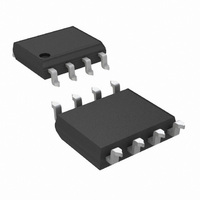
IC REG TERM DDR-I/DDR-II 8SOIC
Manufacturer
National Semiconductor
Datasheet
1.LP2998MRNOPB.pdf
(18 pages)
Specifications of LP2998MAX/NOPB
Applications
Converter, DDR, DDR2, DDR3
Voltage - Input
2.2 ~ 5.5 V
Number Of Outputs
1
Operating Temperature
-40°C ~ 125°C
Mounting Type
Surface Mount
Package / Case
8-SOIC (3.9mm Width)
For Use With
LP2998EVAL - BOARD EVALUATION FOR LP2998
Lead Free Status / RoHS Status
Lead free / RoHS Compliant
Voltage - Output
-
Other names
LP2998MAX
Available stocks
Company
Part Number
Manufacturer
Quantity
Price
Company:
Part Number:
LP2998MAX/NOPB
Manufacturer:
ALLEGRO
Quantity:
16 458
Part Number:
LP2998MAX/NOPB
Manufacturer:
TI/德州仪器
Quantity:
20 000
Block Diagram
Description
The LP2998 is a linear bus termination regulator designed to
meet the JEDEC requirements of SSTL-2 and SSTL-18. The
output, V
regulating the output voltage equal to VDDQ / 2. The output
stage has been designed to maintain excellent load regulation
while preventing shoot through. The LP2998 also incorpo-
rates two distinct power rails that separates the analog cir-
cuitry from the power output stage. This allows a split rail
approach to be utilized to decrease internal power dissipation.
It also permits the LP2998 to provide a termination solution
for the next generation of DDR-SDRAM memory (DDRII). The
LP2998 can also be used to provide a termination voltage for
other logic schemes such as SSTL-3 or HSTL.
Series Stub Termination Logic (SSTL) was created to im-
prove signal integrity of the data transmission across the
memory bus. This termination scheme is essential to prevent
data error from signal reflections while transmitting at high
frequencies encountered with DDR-SDRAM. The most com-
mon form of termination is Class II single parallel termination.
This involves one R
memory and one R
R
scale the current requirements from the LP2998. This imple-
mentation can be seen below in .
S
and R
TT
T
FIGURE 1. SSTL-Termination Scheme
are 25 Ohms, although these can be changed to
is capable of sinking and sourcing current while
T
S
termination resistor. Typical values for
series resistor from the chipset to the
30026906
9
Pin Descriptions
AVIN AND PVIN
AVIN and PVIN are the input supply pins for the LP2998. AVIN
is used to supply all the internal control circuitry. PVIN, how-
ever, is used exclusively to provide the rail voltage for the
output stage used to create V
bility to work off separate supplies, under the condition that
AVIN is always greater than or equal to PVIN. For SSTL-18
applications, it is recommended to connect PVIN to the 1.8V
rail used for the memory core and AVIN to a rail within its
operating range of 2.2V to 5.5V (typically a 2.5V supply). PVIN
should always be used with either a 1.8V or 2.5V rail. This
prevents the thermal limit from tripping because of excessive
internal power dissipation. If the junction temperature ex-
ceeds the thermal shutdown threshold, the part will enter a
shutdown state identical to the manual shutdown where V
is tri-stated and V
1.5V can be used but it will reduce the maximum output cur-
rent. Therefore it is not recommended for most termination
schemes.
VDDQ
VDDQ is the input used to create the internal reference volt-
age for regulating V
from a resistor divider of two internal 50kΩ resistors. This
guarantees that V
implementation of VDDQ is as a remote sense. This can be
achieved by connecting VDDQ directly to the 1.8V rail at the
DIMM instead of PVIN. This ensures that the reference volt-
age precisely tracks the DDR memory rails without a large
voltage drop from the power lines. For SSTL-18 applications,
VDDQ will be a 1.8V signal, which will create a 0.9V termina-
tion voltage at V
exact values of V
V
The purpose of the sense pin is to provide improved remote
load regulation. In most motherboard applications, the termi-
nation resistors will connect to V
voltage was regulated only at the output of the LP2998, then
the long trace will cause a significant IR drop resulting in a
termination voltage lower at one end of the bus than the other.
The V
connecting it to the middle of the bus. This will provide a better
distribution across the entire termination bus. If remote load
regulation is not used, then the V
SENSE
SENSE
pin can be used to improve this performance by
TT
TT
TT
REF
(See Electrical Characteristics Table for
will precisely track VDDQ / 2. The optimal
over temperature).
TT
remains active. A lower rail, such as
. The reference voltage is generated
30026905
TT
TT
. These pins have the capa-
SENSE
in a long plane. If the output
pin must still be con-
www.national.com
TT


