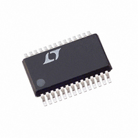
LTC1703CG Linear Technology, LTC1703CG Datasheet - Page 11

LTC1703CG
Manufacturer Part Number
LTC1703CG
Description
IC REG SW DUAL SYNC VID 28SSOP
Manufacturer
Linear Technology
Datasheet
1.LTC1703CG.pdf
(36 pages)
Specifications of LTC1703CG
Applications
Controller, Mobile Intel Pentium® III
Voltage - Input
3 ~ 7 V
Number Of Outputs
2
Voltage - Output
0.9 ~ 2 V
Operating Temperature
0°C ~ 85°C
Mounting Type
Surface Mount
Package / Case
28-SSOP
Lead Free Status / RoHS Status
Contains lead / RoHS non-compliant
Available stocks
Company
Part Number
Manufacturer
Quantity
Price
Part Number:
LTC1703CG
Manufacturer:
LT/凌特
Quantity:
20 000
Part Number:
LTC1703CG#TRPBF
Manufacturer:
LTNEAR
Quantity:
20 000
APPLICATIO S I FOR ATIO
This constant frequency operation brings with it a couple
of benefits. Inductor and capacitor values can be chosen
with a precise operating frequency in mind and the feed-
back loop components can be similarly tightly specified.
Noise generated by the circuit will always be in a known
frequency band with the 550kHz frequency designed to
leave the 455kHz IF band free of interference. Subharmonic
oscillation and slope compensation, common headaches
with constant frequency current mode switchers, are
absent in voltage mode designs like the LTC1703.
During the time that QT is on, its source (the SW pin) is at
V
ever, QT requires V
minimum R
it needs to generate a gate drive signal at TG higher than
its highest supply voltage. To accomplish this, the TG
driver runs from floating supplies, with its negative supply
attached to SW and its power supply at BOOST. This allows
it to slew up and down with the source of QT. In combination
with a simple external charge pump (Figure 2), this allows
the LTC1703 to completely enhance the gate of QT without
requiring an additional, higher supply voltage.
The two channels of the LTC1703 run from a common
clock, with the phasing chosen to be 180° from side 1 to
side 2. This has the effect of doubling the frequency of the
switching pulses seen by the input bypass capacitor,
significantly lowering the RMS current seen by the capaci-
tor and reducing the value required (see the 2-Phase
section).
Feedback Amplifier
Each side of the LTC1703 senses the output voltage at
V
gram). This is a real op amp with a low impedance output,
85dB open-loop gain and 25MHz gain-bandwidth product.
The positive input is connected internally to an 800mV
reference, while the negative input is connected to the FB
pin. The output is connected to COMP, which is in turn
connected to the soft-start circuitry and from there to the
PWM generator.
Unlike many regulators that use a resistor divider con-
nected to a high impedance feedback input, the LTC1703
is designed to use an inverting summing amplifier
IN
OUT
. V
with an internal feedback op amp (see Block Dia-
IN
is also the power supply for the LTC1703. How-
ON
. This presents a problem for the LTC1703—
U
IN
+ V
U
GS(ON)
at its gate to achieve
W
U
topology with the FB pin configured as a virtual ground.
This allows flexibility in choosing pole and zero locations
not available with simple g
it allows the use of “type 3” compensation, which pro-
vides a phase boost at the LC pole frequency and signifi-
cantly improves loop phase margin (see Figure 3). The
Feedback Loop/Compensation section contains a de-
tailed explanation of type 3 feedback loops. Note that side
1 of the LTC1703 includes R1 and R
of the VID DAC circuitry.
MIN/MAX COMPARATORS
Two additional feedback loops keep an eye on the primary
feedback amplifier and step in if the feedback node moves
±5% from its nominal 800mV value. The MAX comparator
(see Block Diagram) activates whenever FB rises more
than 5% above 800mV. It immediately turns the top
MOSFET (QT) off and the bottom MOSFET (QB) on and
keeps them that way until FB falls back within 5% of its
nominal value. This pulls the output down as fast as pos-
sible, preventing damage to the (often expensive) load. If
FB rises because the output is shorted to a higher supply,
QB will stay on until the short goes away, the higher supply
LTC1703
COMP
Figure 3. “Type 3” Feedback Loop (Side 2 Shown)
R2
PV
CC
Figure 2. Floating TG Driver Supply
PGND
FB
BOOST
C2
SW
BG
TG
+
–
0.8V
C1
m
D
C
1µF
configurations. In particular,
CP
FB
CP
V
IN
QT
QB
1703 F03
B
R
L
B
internally as part
R3
EXT
LTC1703
R1
+
+
C3
C
C
OUT
11
IN
V
1703 F02
OUT
1703fa
V
OUT


