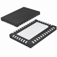
LT3513EUHF#TRPBF Linear Technology, LT3513EUHF#TRPBF Datasheet - Page 19

LT3513EUHF#TRPBF
Manufacturer Part Number
LT3513EUHF#TRPBF
Description
IC REG 5-OUT FOR TFT-LCD 38QFN
Manufacturer
Linear Technology
Datasheet
1.LT3513EUHFPBF.pdf
(22 pages)
Specifications of LT3513EUHF#TRPBF
Applications
Converter, TFT, LCD
Voltage - Input
4.5 ~ 30 V
Number Of Outputs
5
Voltage - Output
0.8 ~ 40 V
Operating Temperature
-40°C ~ 125°C
Mounting Type
Surface Mount
Package / Case
38-QFN
Lead Free Status / RoHS Status
Lead free / RoHS Compliant
Available stocks
Company
Part Number
Manufacturer
Quantity
Price
inverting regulators, the switched currents flow through
the power switch, the switching diode and the tank capaci-
tor. The loop formed by the components in the switched
current path should be as small as possible. Place these
components, along with the inductor and output capacitor,
on the same side of the circuit board, and connect them
on that layer. Place a local, unbroken ground plane below
these components, and tie this ground plane to system
ground at one location, ideally at the ground terminal of
the output capacitor C2. Additionally, keep the SW and
BOOST nodes as small as possible.
operaTion
Figure 3. Subtracting the Current When the Switch is On (3a)
from the Current When the Switch is Off (3b) Reveals the Path of
the High Frequency Switching Current (3c) Keep this Loop Small.
The Voltage on the SW and BOOST Nodes Will Also Be Switched;
Keep These Nodes as Small as Possible. Finally, Make Sure the
Circuit is Shielded with a Local Ground Plane
I
C1
C1
V
V
V
IN
IN
IN
GND
GND
GND
SW
SW
SW
(3a)
(3b)
(3c)
V
SW
D1
L1
3519 F03
C2
Thermal Considerations
The PCB must provide heat sinking to keep the LT3513
cool. The Exposed Pad on the bottom of the package must
be soldered to a ground plane. This ground should be tied
to other copper layers below with thermal vias; these lay-
ers will spread the heat dissipated by the LT3513. Place
additional vias near the catch diodes. Adding more copper
to the top and bottom layers and tying this copper to the
internal planes with vias can reduce thermal resistance
further. With these steps, the thermal resistance from die
(or junction) to ambient can be reduced to θ
or less. With 100LFPM airflow, this resistance can fall
by another 25%. Further increases in airflow will lead to
lower thermal resistance.
Figure 4. Topside PCB Layout
LT3513
JA
19
= 25°C
3513fc


