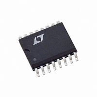
LT1184FCS Linear Technology, LT1184FCS Datasheet - Page 12

LT1184FCS
Manufacturer Part Number
LT1184FCS
Description
IC SW REG CCFL CONTRAST 16-SOIC
Manufacturer
Linear Technology
Datasheet
1.LT1184FCSPBF.pdf
(24 pages)
Specifications of LT1184FCS
Applications
Converter, CCFL, LCD
Voltage - Input
3 ~ 30 V
Number Of Outputs
1
Operating Temperature
0°C ~ 100°C
Mounting Type
Surface Mount
Package / Case
16-SOIC (3.9mm Width)
Lead Free Status / RoHS Status
Contains lead / RoHS non-compliant
Voltage - Output
-
Other names
LT1184FCSW
LT1184FCSW
LT1184FCSW
Available stocks
Company
Part Number
Manufacturer
Quantity
Price
Part Number:
LT1184FCS
Manufacturer:
LINEAR/凌特
Quantity:
20 000
Company:
Part Number:
LT1184FCS#PBF
Manufacturer:
LT
Quantity:
17
Part Number:
LT1184FCS#PBF
Manufacturer:
LINEAR/凌特
Quantity:
20 000
Part Number:
LT1184FCS#TRPBF
Manufacturer:
LINEAR/凌特
Quantity:
20 000
PIN
LT1182/LT1183/LT1184/LT1184F
LCD V
NPN power switch for the LCD contrast regulator. The
power switch provides a minimum of 625mA. Maximum
switch current is a function of duty cycle as internal slope
compensation ensures stability with duty cycles greater
than 50%. Using a driver loop to automatically adapt base
drive current to the minimum required to keep the switch
in a quasi-saturation state yields fast switching times and
high efficiency operation. The ratio of switch current to
driver current is about 50:1.
LT1182
FBN (Pin 10): This pin is the noninverting terminal for the
negative contrast control error amplifier. The inverting
terminal is offset from ground by –12mV and defines the
error amplifier output state under start-up conditions. The
FBN pin acts as a summing junction for a resistor divider
network. Input bias current for this pin is typically 1 A
flowing out of the pin. If this pin is not used, force FBN to
greater than 0.5V to deactivate the negative contrast
control input stage. The proximity of FBN to the LCD V
pin makes it sensitive to ringing on the switch pin. A small
capacitor (0.01 F) from FBN to ground filters switching
ripple.
FBP (Pin 11): This pin is the inverting terminal for the
positive contrast control error amplifier. The noninverting
terminal is tied to an internal 1.244V reference. Input bias
current for this pin is typically 0.5 A flowing into the pin.
If this pin is not used, ground FBP to deactivate the positive
contrast control input stage. The proximity of FBP to the
LCD V
pin. A small capacitor (0.01 F) from FBP to ground filters
switching ripple.
LT1183
FB (Pin 10): This pin is the common connection between
the noninverting terminal for the negative contrast error
12
U
SW
SW
FUNCTIONS
(Pin 9): This pin is the collector of the internal
pin makes it sensitive to ringing on the switch
U
U
SW
amplifier and the inverting terminal for the positive-con-
trast error amplifier. In comparison to the LT1182, the FBN
and the FBP pins tie together and come out as one pin. This
scheme permits one polarity of contrast to be regulated.
The proximity of FB to the LCD V
to ringing on the switch pin. A small capacitor (0.01 F)
from FB to ground filters switching ripple.
generating negative contrast voltages. The pin has two
stable operating points; regulating to 1.244V for positive
contrast voltages or regulating to –12mV for negative
contrast voltages. Under start-up conditions, the FB pin
heads to a positive voltage. If negative contrast voltages
are generated, tie a diode from the FB pin to ground. This
ensures that the FB pin will clamp before reaching the
positive reference voltage. Switching action then pulls the
FB pin back to its normal servo voltage.
LT1183/LT1184/LT1184F
REF (Pin 11): This pin brings out the 1.244V reference. Its
functions include the programming of negative contrast
voltages with an external resistor divider network (LT1183
only) and the programming of lamp current for the I
pin. LTC does not recommend using the REF pin for both
functions at once. The REF pin has a typical output
impedance of 45
impedance of 15
load current should be limited to a few hundred microam-
peres, otherwise reference regulation will be degraded.
REF is used to generate the maximum programming
current for the I
pins. PWM or DAC control subtracts from the maximum
programming current. A small decoupling capacitor (0.1uF)
is recommended to filter switching transients.
The FB pin requires attention to start-up conditions when
CCFL
on the LT1183 and a typical output
on the LT1184/LT1184F. Reference
pin by placing a resistor between the
SW
pin makes it sensitive
CCFL


