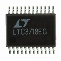
LTC3718EG#PBF Linear Technology, LTC3718EG#PBF Datasheet - Page 10

LTC3718EG#PBF
Manufacturer Part Number
LTC3718EG#PBF
Description
IC DC/DC CONTRLR DDR/QDR 24-SSOP
Manufacturer
Linear Technology
Datasheet
1.LTC3718EG.pdf
(20 pages)
Specifications of LTC3718EG#PBF
Applications
Controller, DDR, QDR
Voltage - Input
1.5 ~ 36 V
Number Of Outputs
1
Voltage - Output
0.75 ~ 18 V
Operating Temperature
-40°C ~ 85°C
Mounting Type
Surface Mount
Package / Case
24-SSOP
Lead Free Status / RoHS Status
Lead free / RoHS Compliant
Available stocks
Company
Part Number
Manufacturer
Quantity
Price
APPLICATIO S I FOR ATIO
LTC3718
A typical LTC3718 application circuit is shown in
Figure 1. External component selection is primarily de-
termined by the maximum load current and begins with
the selection of the sense resistance and power MOSFET
switches. The LTC3718 uses the on-resistance of the
synchronous power MOSFET for determining the induc-
tor current. The desired amount of ripple current and
operating frequency largely determines the inductor value.
Finally, C
RMS current into the converter and C
low enough ESR to meet the output voltage ripple and
transient specification.
Maximum Sense Voltage and V
Inductor current is determined by measuring the voltage
across a sense resistance that appears between the
SENSE
is set by the voltage applied to the V
to approximately (0.13)V
(0.17)V
loop will not allow the inductor current valleys to exceed
(0.13)V
for sinking current. In practice, one should allow some
margin for variations in the LTC3718 and external com-
ponent values and a good guide for selecting the sense
resistance is:
when V
An external resistive divider from INTV
set the voltage of the V
resulting in nominal sense voltages of 50mV to 200mV.
Additionally, the V
in which case the nominal sense voltage defaults to 70mV
or 140mV, respectively. The maximum allowed sense
voltage is about 1.3 times this nominal value for positive
output current and 1.7 times the nominal value for nega-
tive output current.
Connecting the SENSE
The LTC3718 can be used with or without a sense resistor.
When using a sense resistor, it is placed between the
source of the bottom MOSFET M2 and ground. Connect
10
R
SENSE
+
RNG
RNG
RNG
and SENSE
IN
/R
is selected for its ability to handle the large
for sinking current. The current mode control
= 0.5 – 2V.
10 •
SENSE
I
V
OUT MAX
RNG
RNG
U
for sourcing current and (0.17)V
–
(
pins. The maximum sense voltage
pin can be tied to SGND or INTV
+
RNG
and SENSE
U
RNG
)
pin between 0.5V and 2V
for sourcing current and
RNG
W
RNG
–
Pin
OUT
Pins
CC
pin and is equal
can be used to
is chosen with
U
RNG
CC
the SENSE
sense resistor with SENSE
MOSFET and the SENSE
resistor provides a well defined current limit, but adds cost
and reduces efficiency. Alternatively, one can eliminate the
sense resistor and use the bottom MOSFET as the current
sense element by simply connecting the SENSE
drain and the SENSE
MOSFET. This improves efficiency, but one must carefully
choose the MOSFET on-resistance as discussed in a later
section.
Power MOSFET Selection
The LTC3718 requires two external N-channel power
MOSFETs, one for the top (main) switch and one for the
bottom (synchronous) switch. Important parameters for
the power MOSFETs are the breakdown voltage V
threshold voltage V
transfer capacitance C
The gate drive voltage is set by the 5V INTV
Consequently, logic-level threshold MOSFETs must be
used in LTC3718 applications.
When the bottom MOSFET is used as the current sense
element, particular attention must be paid to its
on-resistance. MOSFET on-resistance is typically speci-
fied with a maximum value R
case, additional margin is required to accommodate the
rise in MOSFET on-resistance with temperature:
The
accounting for the significant variation in on-resistance
with temperature, typically about 0.4%/ C as shown in
Figure 2. For a maximum junction temperature of 100 C,
using a value
The power dissipated by the top and bottom MOSFETs
strongly depends upon their respective duty cycles and
the load current. During normal operation, the duty cycles
for the MOSFETs are:
R
DS ON MAX
T
(
term is a normalization factor (unity at 25 C)
)(
+
and SENSE
T
)
= 1.3 is reasonable.
(GS)TH
R
SENSE
RSS
–
–
T
pin to the source of the bottom
pins as a Kelvin connection to the
–
, on-resistance R
and maximum current I
pin to PGND1. Using a sense
+
at the source of the bottom
DS(ON)(MAX)
at 25 C. In this
DS(ON)
CC
+
pin to the
, reverse
DS(MAX)
(BR)DSS
supply.
3718fa
,
.


