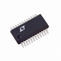
LTC3718EG Linear Technology, LTC3718EG Datasheet - Page 9

LTC3718EG
Manufacturer Part Number
LTC3718EG
Description
IC DC/DC CONTRLR DDR/QDR 24-SSOP
Manufacturer
Linear Technology
Datasheet
1.LTC3718EG.pdf
(20 pages)
Specifications of LTC3718EG
Applications
Controller, DDR, QDR
Voltage - Input
1.5 ~ 36 V
Number Of Outputs
1
Voltage - Output
0.75 ~ 18 V
Operating Temperature
-40°C ~ 85°C
Mounting Type
Surface Mount
Package / Case
24-SSOP
Lead Free Status / RoHS Status
Contains lead / RoHS non-compliant
Available stocks
Company
Part Number
Manufacturer
Quantity
Price
Company:
Part Number:
LTC3718EG
Manufacturer:
LT
Quantity:
2 000
Part Number:
LTC3718EG
Manufacturer:
LT/凌特
Quantity:
20 000
Part Number:
LTC3718EG#PBF
Manufacturer:
LINEAR/凌特
Quantity:
20 000
Company:
Part Number:
LTC3718EG#TRPBF
Manufacturer:
MT
Quantity:
1 255
Part Number:
LTC3718EG#TRPBF
Manufacturer:
LINEAR/凌特
Quantity:
20 000
Company:
Part Number:
LTC3718EGTRPBF
Manufacturer:
LINEAR
Quantity:
594
OPERATIO
Main Control Loop
The LTC3718 is a current mode controller for DC/DC
step-down converters designed to operate from low input
voltages. It incorporates a boost converter with a buck
regulator.
Buck Regulator Operation
In normal operation, the top MOSFET is turned on for a
fixed interval determined by a one-shot timer OST. When
the top MOSFET is turned off, the bottom MOSFET is
turned on until the current comparator I
ing the one-shot timer and initiating the next cycle. Induc-
tor current is determined by sensing the voltage between
the SENSE
on-resistance . The voltage on the I
parator threshold corresponding to inductor valley cur-
rent. The error amplifier EA adjusts this voltage by com-
paring the feedback signal V
with an internal reference generated from one half of the
voltage on V
drop in the feedback voltage relative to the reference. The
I
again matches the load current.
The operating frequency is determined implicitly by the
top MOSFET on-time and the duty cycle required to
maintain regulation. The one-shot timer generates an on-
time that is proportional to the ideal duty cycle, thus
holding frequency approximately constant with changes
in V
external resistor R
Overvoltage and undervoltage comparators OV and UV
pull the PGOOD output low if the output feedback voltage
exits a
Furthermore, in an overvoltage condition, M1 is turned off
and M2 is turned on and held on until the overvoltage
condition clears.
Pulling the RUN/SS pin low forces the controller into its
shutdown state, turning off both M1 and M2. Releasing the
pin allows an internal 1.2 A current source to charge up an
external soft-start capacitor C
1.5V, the controller turns on and begins switching, but
with the I
the RUN/SS voltage. As C
start current limit is removed.
TH
voltage then rises until the average inductor current
IN
. The nominal frequency can be adjusted with an
TH
10% window around the regulation point.
+
voltage clamped at approximately 0.6V below
and SENSE
REF
. If the load current increases, it causes a
U
ON
.
–
pins using the bottom MOSFET
SS
continues to charge, the soft-
SS
FB1
. When this voltage reaches
from the output voltage
TH
pin sets the com-
CMP
trips, restart-
INTV
Power for the top and bottom MOSFET drivers and most
of the internal controller circuitry is derived from the
INTV
floating bootstrap capacitor C
charged from INTV
D
Boost Regulator Operation
The 5V power source for INTV
current mode, internally compensated fixed frequency
step-up switching regulator that has been incorporated
into the LTC3718.
Operation can be best understood by referring to the
Functional Diagrams. Q1 and Q2 form a bandgap refer-
ence core whose loop is closed around the output of the
regulator. The voltage drop across R5 and R6 is low
enough such that Q1 and Q2 do not saturate, even when
V
1.23V, causing V
crease. Comparator A2’s output stays high, keeping switch
Q3 in the off state. As increased output loading causes the
V
current is regulated directly on a cycle-by-cycle basis by
the V
switch cycle, turning on the switch. When the summation
of a signal representing switch current and a ramp gen-
erator (introduced to avoid subharmonic oscillations at
duty factors greater than 50%) exceeds the V
comparator A2 changes state, resetting the flip-flop and
turning off the switch. More power is delivered to the
output as switch current is increased. The output voltage,
attenuated by external resistor divider R7 and R8, appears
at the V
pensation is provided internally by R
response can be optimized by the addition of a phase lead
capacitor C
large value or low ESR output capacitors are used.
As the load current is decreased, the switch turns on for
a shorter period each cycle. If the load current is further
decreased, the boost converter will skip cycles to main-
tain output voltage regulation. If the V
increased significantly above 1.23V, the boost converter
will enter a low power state.
IN2
FB2
B
when the top MOSFET is turned off.
is 1V. When there is no load, V
CC
CC
C
voltage to decrease, A1’s output increases. Switch
node. The flip-flop is set at the beginning of each
FB2
Power
pin. The top MOSFET driver is powered from a
pin, closing the overall loop. Frequency com-
PL
in parallel with R7 in applications where
C
CC
(the error amplifier’s output) to de-
through an external Schottky diode
CC
B
. This capacitor is re-
FB2
can be provided by a
C
rises slightly above
and C
FB2
LTC3718
pin voltage is
C
. Transient
C
signal,
3718fa
9


