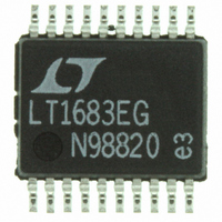
LTC1753CG Linear Technology, LTC1753CG Datasheet - Page 10

LTC1753CG
Manufacturer Part Number
LTC1753CG
Description
IC SW REG CNTRLR PENT III 20SSOP
Manufacturer
Linear Technology
Datasheet
1.LTC1753CGPBF.pdf
(24 pages)
Specifications of LTC1753CG
Applications
Controller, Intel Pentium® III
Voltage - Input
5V
Number Of Outputs
1
Voltage - Output
1.3 ~ 3.5 V
Operating Temperature
0°C ~ 70°C
Mounting Type
Surface Mount
Package / Case
20-SSOP
Lead Free Status / RoHS Status
Contains lead / RoHS non-compliant
Available stocks
Company
Part Number
Manufacturer
Quantity
Price
Company:
Part Number:
LTC1753CG
Manufacturer:
LINEAR
Quantity:
8 192
Part Number:
LTC1753CG#PBF
Manufacturer:
LINEAR/凌特
Quantity:
20 000
Company:
Part Number:
LTC1753CG#TR
Manufacturer:
LT
Quantity:
2 000
FU CTIO TABLES
APPLICATIO S I FOR ATIO
LTC1753
Table 1. PWRGD and FAULT Logic
Table 2. Rated Output Voltage
OVERVIEW
The LTC1753 is a voltage feedback, synchronous switch-
ing regulator controller (see Block Diagram) designed for
use in high power, low voltage step-down (buck) convert-
ers. It includes an on-chip DAC to control the output
voltage, a PWM generator, a precision reference trimmed
to 1%, two high power MOSFET gate drivers and all the
necessary feedback and control circuitry to form a com-
plete switching regulator circuit.
The LTC1753 includes a current limit sensing circuit that
uses the upper external power MOSFET as a current
sensing element, eliminating the need for an external
sense resistor. Once the current comparator, CC, detects
an overcurrent condition, the duty cycle is reduced by
discharging the soft-start capacitor through a voltage-
10
V
ID4
0
0
0
0
0
0
0
0
0
0
0
0
U
OUTEN
0
1
1
1
1
V
ID3
1
1
1
1
1
1
1
1
0
0
0
0
INPUT
U
INPUT PIN
V
V
ID2
1
1
1
1
0
0
0
0
1
1
1
1
< 103%
> 113%
>103%
SENSE
< 97%
> 97%
U
X
**
V
U
ID1
1
1
0
0
1
1
0
0
1
1
0
0
FAULT
V
ID0
1
0
1
0
1
0
1
0
1
0
1
0
W
1
1
1
1
0
OUTPUT*
RATED OUTPUT
VOLTAGE (V)
1.30
1.35
1.40
1.45
1.50
1.55
1.60
1.65
1.70
1.75
1.80
1.85
U
PWRGD
0
0
1
0
0
controlled current source. Under severe overloads or
output short circuit conditions, the chip will be repeatedly
forced into soft-start until the short is removed, prevent-
ing the external components from being damaged. Under
output overvoltage conditions, the MOSFET drivers will be
disabled permanently until the chip power supply is
recycled or the OUTEN pin is toggled.
OUTEN can optionally be connected to an external nega-
tive temperature coefficient (NTC) thermistor placed near
the external MOSFETs or the microprocessor. Two thresh-
old levels are provided internally. When OUTEN drops to
1.7V, the G1 and G2 pins will be forced low. If OUTEN is
pulled below 1.2V, the LTC1753 will go into shutdown
mode, cutting the supply current to a minimum. If thermal
shutdown is not required, OUTEN can be connected to a
Table 2. Rated Output Voltage (cont)
** With respect to the output voltage selected in Table 2
X Don’t care
* With external pull-up resistor
V
ID4
0
0
0
0
1
1
1
1
1
1
1
1
1
1
1
1
1
1
1
1
V
ID3
0
0
0
0
1
1
1
1
1
1
1
1
0
0
0
0
0
0
0
0
INPUT PIN
V
ID2
0
0
0
0
1
1
1
1
0
0
0
0
1
1
1
1
0
0
0
0
V
ID1
1
1
0
0
1
1
0
0
1
1
0
0
1
1
0
0
1
1
0
0
V
ID0
1
0
1
0
1
0
1
0
1
0
1
0
1
0
1
0
1
0
1
0
RATED OUTPUT
VOLTAGE (V)
SHDN
1.90
1.95
2.00
2.05
2.1
2.2
2.3
2.4
2.5
2.6
2.7
2.8
2.9
3.0
3.1
3.2
3.3
3.4
3.5
1753fa


