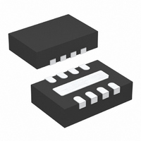
LTC3408EDD Linear Technology, LTC3408EDD Datasheet

LTC3408EDD
Specifications of LTC3408EDD
Available stocks
Related parts for LTC3408EDD
LTC3408EDD Summary of contents
Page 1
... The internal synchronous switch increases efficiency and eliminates the need for an external Schottky diode. The LTC3408 is available in a low profile (0.75mm) 8-lead 3mm × 3mm DFN package. , LTC and LT are registered trademarks of Linear Technology Corporation. U.S. Patent Numbers: 5481178, 6580258, 6304066, 6127815, 6498466, 6611131 4.7µH* V OUT 3× ...
Page 2
... Note calculated from the ambient temperature T J dissipation P according to the following formula: D LTC3408 ORDER PART NUMBER 8 V OUT LTC3408EDD REF 5 RUN DD PART MARKING LAEA = 43°C/ W, θ = 3° 25°C. A MIN TYP MAX ● ...
Page 3
ELECTRICAL CHARACTERISTICS Note 4: When V > 1.2V and V x3 > the P-channel FET will be on REF REF IN in parallel with the bypass PFET reducing the overall R Note 5: This IC includes overtemperature protection ...
Page 4
LTC3408 W U TYPICAL PERFOR A CE CHARACTERISTICS Frequency vs V OUT 1600 T = 25° 3.6V IN 1400 1200 1000 800 600 400 0 0.2 0.4 0.6 0.8 1.0 1.2 V (V) OUT 3408 G08 R ...
Page 5
W U TYPICAL PERFOR A CE CHARACTERISTICS Output Ripple Waveform V OUT 10mV/DIV I L 100mA/DIV V = 3.6V 200ns/DIV 0.6V REF LOAD REF Transient V REF 0.5V/DIV V OUT 1V/DIV V = 4.2V ...
Page 6
LTC3408 CTIO AL DIAGRA OSC FREQ ÷ 2 REF 6 V OUT FB 8 360k V OUT 1 180k – BCMP + 1.2V RUN 5 U OPERATIO (Refer to Functional Diagram) 4.7µ 2. ...
Page 7
U OPERATIO (Refer to Functional Diagram) off and on the bypass P-channel MOSFET with a frequency of approximately 50kHz to 100kHz at 1.6A peak current. This will continue until the short is removed. While the bypass P-channel MOSFET is pulsing ...
Page 8
LTC3408 U U APPLICATIO S I FOR ATIO At output voltages below 0.6V, the switching frequency decreases linearly to a minimum of approximately 700kHz. This places the maximum ripple current (in forced con- tinuous mode) at the highest input voltage ...
Page 9
U U APPLICATIO S I FOR ATIO forced continuous mode, the LTC3408 will actually pull current from the output until the command from V satisfied. On alternate half cyles, this current actually exits the V terminal, potentially causing a rise ...
Page 10
LTC3408 U U APPLICATIO S I FOR ATIO 1 0.1 0.01 V OUT V OUT V OUT V OUT 0. 100 LOAD CURRENT (mA) Figure 4. Power Lost vs Load Current where ...
Page 11
... BOLD LINES INDICATE HIGH CURRENT PATHS Figure 5. Layout Diagram Information furnished by Linear Technology Corporation is believed to be accurate and reliable. However, no responsibility is assumed for its use. Linear Technology Corporation makes no represen- tation that the interconnection of its circuits as described herein will not infringe on existing patent rights 70° ...
Page 12
... Dual (I Monolithic Step-Down Regulator LTC5505 ThinSOT RF Power Detector with Buffered Output and >40dB Dynamic Range Burst Mode is a registered trademark of Linear Technology Corporaton. ThinSOT is a trademark of Linear Technology Corporation. Linear Technology Corporation 12 1630 McCarthy Blvd., Milpitas, CA 95035-7417 (408) 432-1900 FAX: (408) 434-0507 ● ...


