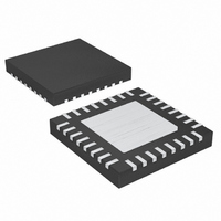
MAX1997ETJ+ Maxim Integrated Products, MAX1997ETJ+ Datasheet - Page 27

MAX1997ETJ+
Manufacturer Part Number
MAX1997ETJ+
Description
IC PWR SUPPLY TFT LCD 32TQFN
Manufacturer
Maxim Integrated Products
Datasheet
1.MAX1997ETJ.pdf
(31 pages)
Specifications of MAX1997ETJ+
Applications
Controller, TFT, LCD
Voltage - Input
2.7 ~ 5.5 V
Number Of Outputs
5
Voltage - Output
2.7 ~ 13 V
Operating Temperature
0°C ~ 85°C
Mounting Type
Surface Mount
Package / Case
32-TQFN Exposed Pad
Lead Free Status / RoHS Status
Lead free / RoHS Compliant
The MAX1997/MAX1998 linear-regulator controllers use
an internal transconductance amplifier to drive an
external pass transistor. The transconductance amplifi-
er, the pass transistor, the base-emitter resistor, and
the output capacitor determine the loop stability.
The transconductance amplifier regulates the output
voltage by controlling the pass transistor’s base cur-
rent. The total DC loop gain is approximately:
where V
transistor’s DC current gain, and I
through the base-to-emitter resistor (R
four linear-regulator controllers is designed for a differ-
ent maximum output current so they have different out-
put drive currents and different bias currents (I
Each controller’s bias current can be found in the
Electrical Characteristics. The current listed in the
Conditions column for the FB_ Regulation Voltage
specification is the individual controller’s bias current.
The base-to-emitter resistor for each controller should
be chosen to set the correct I
The output capacitor and the load resistance create the
dominant pole in the system. However, the internal
amplifier delay, the pass transistor’s input capacitance,
and the stray capacitance at the feedback node create
additional poles in the system, and the output capacitor’s
ESR generates a zero. For proper operation, use the
following steps to ensure the linear regulator stability:
1) First, calculate the dominant pole set by the linear
2) The pole caused by the internal amplifier delay is at
Quintuple/Triple-Output TFT LCD Power Supplies
regulator’s output capacitor and the load resistor:
where C
and R
the maximum load current.
The unity gain crossover of the linear regulator is:
about 1MHz:
T
is 26mV at room temperature, h
LOAD
A
f
CROSSOVER
V(LDO)
LDO
f
POLE(LDO)
is the load resistance corresponding to
is the output capacitance of the LDO
f
______________________________________________________________________________________
POLE(AMP)
=
R
V
BE
4
T
with Fault Protection and VCOM Buffer
= A
+
=
=
1
2πC
I
V(LDO)
BIAS
V
BE
BIAS
≅ 1MHz
I
BIAS FE
Stability Requirements
LDO LOAD
I
LOAD
:
f
1
POLE(LDO)
h
R
BIAS
BE
V
is the current
). Each of the
FE
REF
is the pass
BIAS
).
3) Next, calculate the pole set by the transistor’s input
4) Next, calculate the pole set by the linear regulator’s
5) Next, calculate the zero caused by the output
capacitance, the transistor’s input resistance, and
the base-to-emitter pullup resistor:
Because R
equation can be simplified:
where g
sistor, and f
meters can be found in the transistor’s data sheet.
Therefore, the equation can be further simplified:
feedback resistance and the capacitance between
FB_ and GND (approximately 5pF including stray
capacitance):
and
capacitor’s ESR:
where R
C
LDO
.
m
f
ESR
POLE(CIN)
f
f
f
f
POLE FB N
POLE FB P
POLE FB
POLE FB
is the transconductance of the pass tran-
f
ESR ZERO
BE
T
f
C
R
is the equivalent series resistance of
POLE(CIN)
I
is the transition frequency. Both para-
IN
(
N
(
(
(
is much greater than R
f
_
POLE(CIN)
=
=
)_
)_
)_
)_
R
1
2
2
g
=
=
π
=
=
=
π
m
f
2
=
2
2
2
=
2πC N R
T
π
π
π
π
≈
h
C
2π
g
C
C
C
FE
m
FB
FB
FB
FB
2
=
I
C
π
(
(
(
(
(
R
LDO ESR
C R
h
R
R
R
f
1
1
1
1
88
FE
T
11
16
1
I
19
1
BE
1
N N
R
||
||
||
||
I
II
R
R
R
R
12
17
99
20
R
IN
)
)
)
)
IN
)
, the above
27


