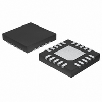
MAX1513ETP+ Maxim Integrated Products, MAX1513ETP+ Datasheet - Page 21

MAX1513ETP+
Manufacturer Part Number
MAX1513ETP+
Description
IC CNTRLR TFT-LCD PS 20-TQFN
Manufacturer
Maxim Integrated Products
Datasheet
1.MAX1513ETP.pdf
(28 pages)
Specifications of MAX1513ETP+
Applications
Controller, TFT, LCD
Voltage - Input
2.7 ~ 5.5 V
Number Of Outputs
1
Voltage - Output
2.7 ~ 50 V
Operating Temperature
-40°C ~ 85°C
Mounting Type
Surface Mount
Package / Case
20-TQFN Exposed Pad
Lead Free Status / RoHS Status
Lead free / RoHS Compliant
In the circuits of Figures 1 and 2, the maximum total
voltage ripple is 1% (peak-to-peak) of the 15V output,
which corresponds to 150mV peak-to-peak ripple. A
conservative way to calculate the maximum ESR and
minimum capacitance is to assume the ESR ripple and
the capacitive ripple each should not exceed 50% of
the total ripple budget.
where V
ple. Since the peak inductor current calculated in the
Inductor Selection section is 2.6A, the maximum ESR of
the output capacitor should be less than 29mΩ. On the
other hand, only 3.1µF capacitance is needed to meet
the capacitive ripple requirement based on the calcula-
tion. A 10µF AQU-series POSCAP with maximum ESR
of 20mΩ is selected for the typical operating circuits in
Figures 1 and 2, which meets both the voltage-ripple
and minimum capacitance requirements.
The typical load on the step-up regulator for source-
driver applications is a large pulsed load, with a peak
current of approximately 1A and a pulse width of
approximately 2µs. The shape of the pulse is close to
triangular, so it is equivalent to a square pulse with 1A
height and 1µs pulse width. The total voltage dip during
the pulsed load transient also has two components: the
ohmic dip due to the output capacitor’s ESR and the
capacitive dip caused by discharging the output
capacitance:
where I
is the pulse width. Higher capacitance and lower ESR
result in less voltage dip. Again, assume the ESR dip
and the capacitive dip each should not exceed 50% of
the total maximum allowed output-voltage dip caused
by a load pulse (V
C
OUT MIN
PULSE
RIPPLE(MAX)
C
OUT MIN
(
V
V
V
(
is the height of the pulse load and t
R
)
DIP
DIP ESR
DIP C
R
ESR MAX
ESR MAX
≥
(
( )
)
DIP(MAX)
______________________________________________________________________________________
=
(
V
(
≥
is the total peak-to-peak output rip-
RIPPLE MAX
2
)
≈
V
DIP ESR
2
×
=
)
I
)
PULSE
×
I
(
MAIN
≤
I
).
PULSE
≤
(
I
PULSE
2
V
V
)
C
V
DIP MAX
RIPPLE MAX
2
DIP MAX
×
OUT
)
+
×
TFT-LCD Power-Supply Controllers
×
(
×
I
×
(
V
t
PULSE
PULSE
DIP C
I
⎛
⎜
⎝
×
PEAK
R
V
(
ESR
V
MAIN
)
( )
t
)
MAIN
PULSE
)
×
-
f
OSC
V
IN
PULSE
For the typical load pulse described above, assuming the
voltage dip must be limited to 200mV, the minimum out-
put capacitor is 10µF, and the maximum ESR is 100mΩ.
The voltage rating and temperature characteristics of
the output capacitor must also be considered.
The input capacitor (C
drawn from the input supply and reduces noise injec-
tion into the device. A 22µF ceramic capacitor is used
in the typical operating circuit (Figure 1) because of the
high source impedance seen in typical lab setups.
Actual applications usually have much lower source
impedance since the step-up regulator often runs
directly from the output of another regulated supply.
Typically, C
the typical operating circuit. Ensure a low noise supply
at IN by using adequate C
age variation can be tolerated on C
from C
in Figure 1).
The MAX1513/MAX1514s’ high switching frequency
demands a high-speed rectifier. Schottky diodes are
recommended for most applications because of their
fast recovery time and low forward voltage. In general,
use a Schottky diode with a current rating exceeding
the peak inductor current calculated in the Inductor
Selection section.
The output voltage of the main step-up regulator is
adjustable by connecting a resistive voltage-divider
from the output (V
with the center tap connected to FB (see Figure 1).
Select R2 in the 10kΩ to 50kΩ range. Calculate R1 with
the following equations:
where V
is 1.25V. Connect the divider close to the IC.
The step-up regulator controller of the MAX1513/
MAX1514 uses a peak current-mode control method.
The loop stability of a current-mode step-up regulator
can be analyzed using a small-signal model. In contin-
uous-conduction mode, the loop-gain transfer function
consists of a DC loop gain, a dominant pole, a right-
half-plane (RHP) zero and an ESR zero.
IN
FB
using an RC lowpass filter (see R11 and C10
, the step-up regulator’s feedback set point,
IN
Output-Capacitor Stability Requirement
can be reduced below the values used in
R
1
=
MAIN
R
2
IN
) to the analog ground plane
×
) reduces the current peaks
⎛
⎜
⎝
IN
Input-Capacitor Selection
Output-Voltage Selection
V
. Alternately, greater volt-
MAIN
V
FB
IN
-
if IN is decoupled
1
⎞
⎟
⎠
Rectifier Diode
21


