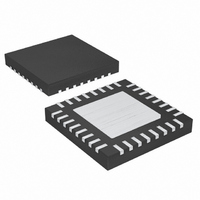
MAX8795AETJ+ Maxim Integrated Products, MAX8795AETJ+ Datasheet - Page 24

MAX8795AETJ+
Manufacturer Part Number
MAX8795AETJ+
Description
IC DC-DC CONV W/OP AMP 32TQFN
Manufacturer
Maxim Integrated Products
Datasheet
1.MAX8795AETJ.pdf
(31 pages)
Specifications of MAX8795AETJ+
Applications
Converter, TFT, LCD
Voltage - Input
2.5 ~ 6 V
Number Of Outputs
8
Voltage - Output
2.5 ~ 18 V
Operating Temperature
-40°C ~ 85°C
Mounting Type
Surface Mount
Package / Case
32-TQFN Exposed Pad
Lead Free Status / RoHS Status
Lead free / RoHS Compliant
and gate-off linear-regulator controllers are 0.1mA.
Therefore, the base-to-emitter resistor for both linear
regulators should be chosen to set 0.1mA bias current:
The output capacitor and the load resistance create the
dominant pole in the system. However, the internal
amplifier delay, pass transistor’s input capacitance,
and the stray capacitance at the feedback node create
additional poles in the system, and the output capaci-
tor’s ESR generates a zero. For proper operation, use
the following equations to verify the linear regulator is
properly compensated:
1) First, determine the dominant pole set by the linear
The unity-gain crossover of the linear regulator is:
2) The pole created by the internal amplifier delay is
3) Next, calculate the pole set by the transistor’s input
g
is the transition frequency. Both parameters can be found
in the transistor’s data sheet. Because RBE is much
greater than RIN, the above equation can be simplified:
Substituting for CIN and RIN yields:
TFT-LCD DC-DC Converter with
Operational Amplifiers
24
m
regulator’s output capacitor and the load resistor:
approximately 1MHz:
capacitance, the transistor’s input resistance, and
the base-to-emitter pullup resistor:
where
is the transconductance of the pass transistor, and f
______________________________________________________________________________________
:
f
POLE LR
f
CROSSOVER
f
R
POLE IN
BE
_
f
C
POLE IN
=
IN
f
_
POLE_AMP
0 1
=
f
=
V
.
POLE IN
_
2π
BE
=
mA
2π
g
2π
×
= A
m
=
f
C
T
_
I
=
×
2π
LOAD MAX LR
OUT LR
,
V_LR
C
0 1
0 7
R
= 1MHz
.
×
=
IN
.
IN
mA
C
h
_
V
×
(
f
IN
FE
1
T
=
1
(
R
×
≈
f
BE
h
×
POLE_LR
g
R
FE
6 8
)_
m
V
IN
. Ω
OUT LR
||
k
R
IN
_
)
T
4) Next, calculate the pole set by the linear regulator’s
where CFB is the capacitance between FB_ and
AGND, R
lator’s feedback divider, and R
tor of the divider.
5) Next, calculate the zero caused by the output
where RESR is the equivalent series resistance of
COUT_LR.
To ensure stability, choose C
the crossover occurs well before the poles and zero
calculated in steps 2 to 5. The poles in steps 3 and 4
generally occur at several megahertz, and using
ceramic capacitors ensures the ESR zero occurs at
several megahertz as well. Placing the crossover below
500kHz is sufficient to avoid the amplifier-delay pole
and generally works well, unless unusual component
choices or extra capacitances move one of the other
poles or the zero below 1MHz.
An IC’s maximum power dissipation depends on the
thermal resistance from the die to the ambient environ-
ment and the ambient temperature. The thermal resis-
tance depends on the IC package, PCB copper area,
other thermal mass, and airflow.
The MAX8795A, with its exposed backside paddle sol-
dered to 1in
plane layer, can dissipate approximately 2.76W into
+70°C still air. More PCB copper, cooler ambient air,
and more airflow increase the possible dissipation, while
less copper or warmer air decreases the IC’s dissipation
capability. The major components of power dissipation
are the power dissipated in the step-up regulator and
the power dissipated by the operational amplifiers.
feedback resistance and the capacitance between
FB_ and AGND (including stray capacitance):
capacitor’s ESR:
f
POLE FB
UPPER
f
POLE ESR
2
_
of PCB copper and a large internal ground
Applications Information
_
is the upper resistor of the linear regu-
=
2π
×
=
C
2π
FB
×
×
C
(
R
OUT LR
OUT_LR
LOWER
UPPER
Power Dissipation
1
1
_
||
×
is the lower resis-
large enough so
R
R
LOWER
ESR
)


