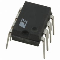
DPA423PN Power Integrations, DPA423PN Datasheet - Page 20

DPA423PN
Manufacturer Part Number
DPA423PN
Description
IC CONV DC-DC DPA SWITCH 8DIP
Manufacturer
Power Integrations
Series
DPA-Switch®r
Specifications of DPA423PN
Applications
Converter, Power Over Ethernet and Telecom Applications
Voltage - Input
16 ~ 75 V
Number Of Outputs
1
Voltage - Output
220V
Operating Temperature
-40°C ~ 125°C
Mounting Type
Through Hole
Package / Case
8-DIP (0.300", 7.62mm)
Output Voltage
9 V
Output Current
1.75 A
Input Voltage
- 0.3 V to + 220 V
Switching Frequency
282 KHz to 425 KHz
Operating Temperature Range
- 40 C to + 150 C
Mounting Style
Through Hole
Duty Cycle (max)
79 %
For Use With
596-1009 - KIT DESIGN ACCELERATOR DC-DC596-1007 - KIT DESIGN ACCELERATOR POE CONV
Lead Free Status / RoHS Status
Lead free / RoHS Compliant
Other names
596-1011-5
Available stocks
Company
Part Number
Manufacturer
Quantity
Price
Part Number:
DPA423PN
Manufacturer:
POWER
Quantity:
20 000
the input decoupling capacitor. The SOURCE pin should not
be used to return the power currents; incorrect operation of the
device may result. The SOURCE is only intended as a signal
ground. The device tab (SOURCE) is the correct connection
for high current with the R package and S-PAK.
The CONTROL pin bypass capacitor should be located as
close as possible to the SOURCE and CONTROL pins and its
SOURCE connection trace should not be shared by the main
MOSFET switching currents. All SOURCE pin referenced
components connected to the LINE-SENSE or EXTERNAL
CURRENT LIMIT pins should also be located closely between
their respective pin and SOURCE. Once again, the SOURCE
connection trace of these components should not be shared
by the main MOSFET switching currents. It is critical that
the tab (SOURCE) power switching currents are returned to the
input capacitor through a separate trace that is not
shared by the components connected to CONTROL,
LINE-SENSE or EXTERNAL CURRENT LIMIT pins.
Any traces to the L or X pins should be kept as short as possible
and away from the DRAIN trace to prevent noise coupling.
LINE-SENSE resistor (R1 in Figure 25) should be located close
to the L pin to minimize the trace length on the L pin side.
In addition to the CONTROL pin capacitor (C6 in Figure 25),
a high frequency bypass capacitor in parallel is recommended
as close as possible between SOURCE and CONTROL pins for
better noise immunity. The feedback optocoupler output should
also be located close to the CONTROL and SOURCE pins of
DPA-Switch.
Heat Sinking
To maximize heat sinking of the DPA-Switch S, R or G package
and the other power components, special thermally conductive
PC board material (aluminum clad PC board) is recommended.
This has an aluminum sheet bonded to the PC board during
the manufacturing process to provide heat sinking directly
and allow the attachment of an external heat sink. If normal
PC board material is used (such as FR4), providing copper
areas on both sides of the board and using thicker copper will
improve heat sinking.
If an aluminum clad board is used then shielding of switching
nodes is recommended. This consists of an area of copper placed
directly underneath switching nodes such as the drain node,
and output diode to provide an electrostatic shield to prevent
coupling to the aluminum substrate. These areas are connected
to input negative in the case of the primary and output return
for secondary. This reduces the amount of capacitive coupling
into the insulated aluminum substrate that can then appear on
the output as ripple and high frequency noise.
20
DPA423-426
P
7/05
Quick Design Checklist
As with any power supply design, all DPA-Switch designs
should be verified on the bench to make sure that component
specifications limits are not exceeded under worst case
conditions. The following minimum set of tests for DPA-Switch
forward converters is strongly recommended:
1. Maximum drain voltage – Verify that peak V
2. Transformer reset margin – Drain voltage should also be
3. Maximum drain current – At maximum ambient temperature,
4. Thermal check – At maximum output power, minimum
Design Tools
Up-to-date information on design tools is available at the Power
Integrations website: www.powerint.com.
exceed minimum BV
maximum overload output power. It is normal, however, to
have additional margin of approximately 25 V below BV
to allow for other power supply component unit-to-unit
variations. Maximum overload output power occurs when
the output is loaded to a level just before the power supply
goes into auto-restart (loss of regulation).
checked at highest input voltage with a severe load step
(50-100%) to verify adequate transformer reset margin. This
test shows the duty cycle at high input voltage, placing the
most demand on the transformer reset circuit.
maximum input voltage and maximum output load, verify
drain current waveforms at start-up for any signs of
transformer or output inductor saturation and excessive
leading edge current spikes. DPA-Switch has a leading edge
blanking time of 100 ns to prevent premature termination
of the on cycle. Verify that the leading edge current spike
does not extend beyond the blanking period.
input voltage and maximum ambient temperature, verify
that temperature specifications are not exceeded for the
transformer, output diodes, output choke(s) and output
capacitors. The DPA-Switch is fully protected against over-
temperature conditions by its thermal shutdown feature. It
is recommended that sufficient heat sinking is provided
to keep the tab temperature at or below 115 °C (S and R
packages), SOURCE pins at or below 100 °C (P/G packages)
under worst case continuous load conditions (at low input
voltage, maximum ambient and full load). This provides
adequate margin to minimum thermal shutdown temperature
(130 °C) to account for part-to-part R
monitoring device temperatures, note that the junction-
to-case thermal resistance should be accounted for when
estimating die temperature.
DSS
at highest input voltage and
DS(ON)
variation. When
DS
does not
DSS


