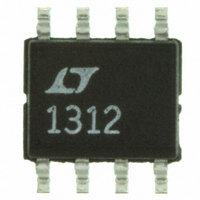
LT1312CS8 Linear Technology, LT1312CS8 Datasheet - Page 6

LT1312CS8
Manufacturer Part Number
LT1312CS8
Description
IC DRVR/REG PCMCIA VPP SNGL8SOIC
Manufacturer
Linear Technology
Datasheet
1.LT1312CS8.pdf
(12 pages)
Specifications of LT1312CS8
Applications
PCMCIA Driver/Regulator, PCMCIA Card Slot
Voltage - Input
13 ~ 20 V
Number Of Outputs
1
Voltage - Output
3.3V, 5V, 12V
Operating Temperature
0°C ~ 70°C
Mounting Type
Surface Mount
Package / Case
8-SOIC (3.9mm Width)
Lead Free Status / RoHS Status
Contains lead / RoHS non-compliant
Available stocks
Company
Part Number
Manufacturer
Quantity
Price
Company:
Part Number:
LT1312CS8
Manufacturer:
LT
Quantity:
10 000
Part Number:
LT1312CS8#PBF
Manufacturer:
LINEAR/凌特
Quantity:
20 000
Part Number:
LT1312CS8#TRPBF
Manufacturer:
LINEAR/凌特
Quantity:
20 000
OPERATION
APPLICATIONS
LT1312
The LT1312 is a programmable output voltage, low-
dropout linear regulator designed specifically for PCMCIA
VPP drive applications. Input power is typically obtained
from a loosely regulated input supply between 13V and
20V (see Applications Information section for more detail
on the input power supply). The LT1312 consists of the
following blocks:
Low Dropout Voltage Linear Regulator: The heart of the
LT1312 is a PNP-based low-dropout voltage regulator
which drops the unregulated supply voltage from 13V to
20V down to 12V, 5V, 3.3V, 0V or Hi-Z depending upon the
state of the two Enable inputs and the V
regulator has built-in current limiting and thermal shut-
down to protect the device, the load, and the socket
against inadvertent short circuiting to ground.
The LT1312 is a voltage programmable linear regulator
designed specifically for PCMCIA VPP driver applications.
The device operates with very low quiescent current
(30 A) in the 0V and Hi-Z modes of operation. In the Hi-Z
mode, the output leakage current falls to 1 A. Unloaded
quiescent current rises to only 55 A and 75 A when
programmed to 3.3V and 5V respectively. In addition to
the low quiescent currents, the LT1312 incorporates sev-
eral protection features which make it ideal for PCMCIA
applications. The LT1312 has built-in current limiting
(330mA) and thermal shutdown to protect the device and
the socket VPP pins against inadvertent short-circuit
conditions.
AUXILIARY WINDING POWER SUPPLIES
Because the LT1312 provides excellent output regulation,
the input power supply may be loosely regulated. One
convenient (and economic) source of power is an auxiliary
winding on the main 5V switching regulator inductor in the
main system power supply.
LTC
Figure 1 is a schematic diagram which describes how a
loosely regulated 14V power supply is created by adding
6
®
1142HV Auxiliary Winding Power Supply
U
U
INFORMATION
U
W
CC
Sense input. The
U
Voltage Control Logic: The LT1312 has five possible
output modes: 0V, 3.3V, 5V, 12V and Hi-Z. These five
modes are selected by the two Enable inputs and the V
Sense input as described by the Truth Table.
V
the LT1312 automatically adjusts the regulated VPP out-
put voltage to 3.3V or 5V depending upon the voltage
present at the PC card V
voltage for the comparator is set at 4V and there is
approximately 50mV of hysteresis provided to ensure
clean switching between 3.3V and 5V.
VPP VALID Comparator: A voltage comparator monitors
the output voltage when the 12V mode is selected and is
driven low when the output is in regulation above 11V.
an auxiliary winding to the 5V inductor in a split 3.3V/5V
LTC1142HV power supply system. A turns ratio of 1:1.8 is
used for transformer T1 to ensure that the input voltage to
the LT1312 falls between 13V and 20V under all load
conditions. The 9V output from this additional winding is
rectified by diode D2, added to the main 5V output and
applied to the input of the LT1312. (Note that the auxiliary
winding must be phased properly as shown in Figure 1.)
The auxiliary winding is referenced to the 5V output which
provides DC current feedback from the auxiliary supply to
the main 5V section. The AC transient response is im-
proved by returning the negative lead of C5 to the 5V
output as shown.
When the 12V output is activated by a TTL high on the
Enable line, the 5V section of the LTC1142HV is forced into
continuous mode operation. A resistor divider composed
of R2, R3 and switch Q3 forces an offset which is sub-
tracted from the internal offset at the Sense
of the LTC1142HV. When this external offset cancels the
built-in 25mV offset, Burst Mode
and the LTC1142HV is forced into continuous mode
operation. (See the LTC1142HV data sheet for further
detail). In this mode, the 14V auxiliary supply can be
Burst Mode is a trademark of Linear Technology Corporation.
CC
Sense Comparator: When the V
CC
supply pin. The threshold
TM
operation is inhibited
CC
mode is selected,
–
input (pin 14)
CC


