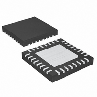
MAX1585ETJ+ Maxim Integrated Products, MAX1585ETJ+ Datasheet - Page 24

MAX1585ETJ+
Manufacturer Part Number
MAX1585ETJ+
Description
IC DGTL CAM PWR SUP 5CH 32TQFN
Manufacturer
Maxim Integrated Products
Datasheet
1.MAX1585ETJ.pdf
(29 pages)
Specifications of MAX1585ETJ+
Applications
Controller, Digital Camera
Voltage - Input
0.7 ~ 5.5 V
Number Of Outputs
5
Voltage - Output
1.25 ~ 5.5 V
Operating Temperature
-40°C ~ 85°C
Mounting Type
Surface Mount
Package / Case
32-TQFN Exposed Pad
Lead Free Status / RoHS Status
Lead free / RoHS Compliant
If the load current is very low (40mA or less), discontin-
uous current is preferred for simple loop compensation
and freedom from duty-cycle restrictions on the inverter
input-output ratio. To ensure discontinuous operation,
the inductor must have a sufficiently low inductance to
fully discharge on each cycle. This occurs when:
A discontinuous current inverter has a single pole at:
Choose the integrator cap so the unity-gain crossover,
f
circuits that do not require fast transient response, it is
often acceptable to overcompensate by setting f
f
C
where:
K = 2L x f
age ramp of 1.25V.
The C
Continuous inductor current may be more suitable for
larger load currents (50mA or more). It improves effi-
ciency by lowering the ratio between peak inductor cur-
rent and output current. It does this at the expense of a
larger inductance value that requires larger size for a
given current rating. With continuous inductor-current
inverter operation, there is a right-half-plane zero,
Z
where D = |V
There is a complex pole pair at:
If the zero due to the output-capacitor capacitance and
ESR is less than 1/10 the right-half-plane zero:
Then choose C
at Z
crossover.
5-Channel Slim DSC Power Supplies
24
C
C
OSC
C
RHP
C
, occurs at f
C
C
is then determined by the following:
= [V
COUT
= (V
______________________________________________________________________________________
/ 20 or lower.
, at:
Z
C
(2π x f
L < [V
COUT
Z
R
IN
Z
COUT
IN
C
RHP
. The ESR zero provides a phase boost at
OSC
/ (K
zero then is used to cancel the f
/ V
C
IN
R
OUT
= 1 / (2π x C
f
MAX1585 AUX2 Inverter Compensation,
MAX1585 AUX2 Inverter Compensation,
)]
)]
OSC
P
RAMP
1/2
C
= [(1 - D)
f
C
/ (|V
/ R
0
= 2 / (2π x R
= (R
| / (|V
so the crossover frequency, f
x V
= (1 - D) / (2π(L x C)
LOAD,
/ 10 or lower. Note that for many AUX
OUT
)[V
RAMP
LOAD
Discontinuous Inductor Current
OUT
REF
| + V
2
and V
Continuous Inductor Current
/ D] x R
OUT
][V
| + V
/ (V
x C
IN
LOAD
REF
)]
REF
OUT
x R
IN
RAMP
2
) (in an inverter).
LOAD
R
/ (V
ESR
) / (2 C
+ |V
x C
LOAD
OUT
is the internal volt-
) < Z
OUT
1/2
OUT
/ (2π x L)
)
/ (2f
C
+ V
)
RHP
|)][g
)
P
OSC
REF
pole, so:
M
/ 10
C,
)] [g
)
/ (2π x
occurs
C
M
at
/
Choose R
C
If Z
ceramic output capacitors) and continuous conduction
is required, then cross the loop over before Z
In that case:
Place:
Or, reduce the inductor value for discontinuous operation.
Any AUX channel can be used for a wide variety of
step-up applications. These include generating 5V or
some other voltage for motor or actuator drive, generat-
ing 15V or a similar voltage for LCD bias, or generating
a step-up current source to efficiently drive a series
array of white LEDs to display backlighting. Figures 5
and 6 show examples of these applications.
Some applications require multiple voltages from a sin-
gle converter channel. This is often the case when gen-
erating voltages for CCD bias or LCD power. Figure 7
shows a two-output flyback configuration with AUX_.
The controller drives an external MOSFET that switches
the transformer primary. Two transformer secondaries
generate the output voltages. Only one positive output
voltage can be fed back, so the other voltages are set
by the turns ratio of the transformer secondaries. The
load stability of the other secondary voltages depends
on transformer leakage, inductance, and winding resis-
tance. Voltage regulation is best when the load on the
secondary that is not fed back is small compared to the
load on the one that is fed back. Regulation also
improves if the load current range is limited. Consult
the transformer manufacturer for the proper design for
a given application.
C
C
C
1 / (2π x R
), at f
COUT
= (V
LED, LCD, and Other Boost Applications
IN
0
to cancel one of the pole pairs:
is not less than Z
C
/ V
R
C
to place the integrator zero, 1 / (2π x R
C
f
RAMP
C
x C
Multiple-Output Flyback Circuits
= (L x C
< f
Applications Information
R
C
0
)[V
C
) = 1 / (2π x R
/ 10, and f
= R
REF
OUT
LOAD
/ (V
)
1/2
RHP
REF
x C
C
/ [(1 - D) x C
< Z
+ |V
LOAD
/ 10 (as is typical with
OUT
RHP
OUT
/ C
x C
/ 10
|)][g
C
OUT
C
M
]
RHP
), so that
/ (2π x f
and f
C
C
0
)]
x
:


