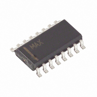
MAX848ESE+ Maxim Integrated Products, MAX848ESE+ Datasheet

MAX848ESE+
Specifications of MAX848ESE+
Related parts for MAX848ESE+
MAX848ESE+ Summary of contents
Page 1
... Pin Configuration appears at end of data sheet. Dual Mode is a trademark of Maxim Integrated Products. ________________________________________________________________ Maxim Integrated Products For free samples & the latest literature: http://www.maxim-ic.com, or phone 1-800-998-8800. For small orders, phone 408-737-7600 ext. 3468. 1-Cell to 3-Cell, High-Power, ...
Page 2
High-Power, Low-Noise, Step-Up DC-DC Converters ABSOLUTE MAXIMUM RATINGS ON1, ON2, OUT, POUT to GND..................................-0.3V, +6V PGND to GND ..........................................................-0.3V, +0. PGND ...............................................-0.3V, (V CLK/SEL, DATA, POKIN, REF, AINSEL, AIN1, AIN2, FB, POK to GND .....-0.3V, ...
Page 3
Low-Noise, Step-Up DC-DC Converters ELECTRICAL CHARACTERISTICS (continued) = 3.6V, GND = PGND = CLK/SEL = ON1 = ON2 = AINSEL = AIN1 = AIN2 = FB = POKIN, POUT = OUT OUT unless otherwise noted.) PARAMETER Operating Current ...
Page 4
High-Power, Low-Noise, Step-Up DC-DC Converters ELECTRICAL CHARACTERISTICS = 3.6V, GND = PGND = CLK/SEL = ON1 = ON2 = AINSEL = AIN1 = AIN2 = FB = POKIN, POUT = OUT OUT unless otherwise noted.) ...
Page 5
Low-Noise, Step-Up DC-DC Converters (T = +25°C, unless otherwise noted.) A MAX849 EFFICIENCY vs. LOAD CURRENT (V = 3.3V) OUT 100 PFM PWM ...
Page 6
High-Power, Low-Noise, Step-Up DC-DC Converters (T = +25°C, unless otherwise noted.) A HEAVY-LOAD SWITCHING WAVEFORMS (V = 3.3V) OUT MAX848/9 TOC- s/div V = 1.1V 200mA 3.3V IN OUT ...
Page 7
Low-Noise, Step-Up DC-DC Converters (T = +25°C, unless otherwise noted.) A MAX849 GSM LOAD-TRANSIENT RESPONSE A B 1ms/div V = 3.6V 5V 440 F IN OUT OUT RIPPLE, 200mV/div, AC COUPLED OUT B ...
Page 8
High-Power, Low-Noise, Step-Up DC-DC Converters PIN NAME 1 AIN1 ADC’s Channel 1 Input. Analog input voltage range is 0.625V to 1.875V. 2 AIN2 ADC’s Channel 2 Input. Analog input voltage range 2.5V. 3 REF ...
Page 9
Low-Noise, Step-Up DC-DC Converters OUT 2.25V ON1 ON ON2 REF 1.25V GND CLK/SEL FB FEEDBACK AND POWER-GOOD SELECT POKIN AINSEL AIN1 AIN2 Figure 1. Functional Diagram _______________Detailed Description The MAX848/MAX849 combine a switching regulator, N-channel power MOSFET, P-channel synchronous rectifier, ...
Page 10
High-Power, Low-Noise, Step-Up DC-DC Converters 10 * OUT POUT C2 MBR0520L MAX849 0 GND 100k L1 POK 0.1 F ON1 LX ON2 PGND CLK/SEL C3 FB 0.22 F POKIN REF * Figure ...
Page 11
Low-Noise, Step-Up DC-DC Converters FEEDBACK REF PWM-MODE CURRENT- LIMIT LEVEL OSC Figure 4. Controller Block Diagram in PWM Mode where V = 1.25V the desired output volt- REF OUT age, and V is the desired ...
Page 12
High-Power, Low-Noise, Step-Up DC-DC Converters f /2 OSC DATA Figure 7. Bit Stream at 1/2 Full Scale When using two counters of the same length, as shown in Figure 8, one counter (A) just counts the A/D ...
Page 13
Low-Noise, Step-Up DC-DC Converters 1M MAX848 MAX849 ON2 OUT ON1 1M Figure 9. Momentary Pushbutton On/Off Switch Capacitor Selection Input Bypass Capacitors A 22µF, low-ESR input capacitor will reduce peak cur- rents and reflected noise due to inductor current ripple. ...
Page 14
High-Power, Low-Noise, Step-Up DC-DC Converters MAX848 MAX849 OUT R POK C Figure 11. Power-On Reset Delay Power-On Reset Delay Adding a timing capacitor from POK to GND generates a power-on reset delay. The reset time constant is ...
Page 15
Low-Noise, Step-Up DC-DC Converters Pin Configuration TOP VIEW 1 16 AIN1 2 15 AIN2 3 14 REF MAX848 4 13 GND MAX849 5 OUT 12 11 POKIN POK 8 Narrow SO ______________________________________________________________________________________ 1-Cell to 3-Cell, ...
Page 16
... Maxim cannot assume responsibility for use of any circuitry other than circuitry entirely embodied in a Maxim product. No circuit patent licenses are implied. Maxim reserves the right to change the circuitry and specifications without notice at any time. 16 ____________________Maxim Integrated Products, 120 San Gabriel Drive, Sunnyvale, CA 94086 408-737-7600 © 1998 Maxim Integrated Products NOTES Printed USA is a registered trademark of Maxim Integrated Products ...


