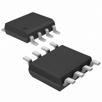
MAX1810ESA+ Maxim Integrated Products, MAX1810ESA+ Datasheet - Page 6

MAX1810ESA+
Manufacturer Part Number
MAX1810ESA+
Description
IC REG SMART NIC 8-SOIC
Manufacturer
Maxim Integrated Products
Datasheet
1.MAX1810ESA.pdf
(8 pages)
Specifications of MAX1810ESA+
Applications
Network, Telecom
Voltage - Input
4.5 ~ 5.5 V
Number Of Outputs
1
Voltage - Output
3.3V
Operating Temperature
-40°C ~ 85°C
Mounting Type
Surface Mount
Package / Case
8-SOIC (3.9mm Width)
Lead Free Status / RoHS Status
Lead free / RoHS Compliant
Network Interface Card Smart Regulator
Figure 1. Functional Diagram
Figure 2. MAIN, STBY, and AUX Transition Voltages
6
_______________________________________________________________________________________
MAIN
STBY
AUX
4.1V(TYP)
INPUT VOLTAGE
MAIN OR STBY
4.475V
3.925V
DET
DET
3.3V
DET
5V
5V
5.5V
0
CONTROL
MAIN
LOGIC
STBY
REG
REG
(IF AUX > 2.5V)
MAIN OR STBY
GUARANTEED
AUX SWITCH
GUARANTEED
GND
THRESHOLD
DETECTION
RANGE
LDO
ON
ON
3.3V
OUT
The MAX1810 powers NICs, modem cards, or other
devices that utilize both the main and auxiliary power
supplies in a PCI-compliant system, or other systems
that utilize a standby or sleep-mode power bus. The
MAX1810 supplies a 3.3V, 500mA output from one of
three inputs: a +5V main, a +5V standby, and a +3.3V
auxiliary voltage.
Each input is separately monitored (Figure 1). During
normal operation, the MAIN input powers the fixed
+3.3V output (OUT) through an internal linear regulator.
When MAIN falls below +4.1V or is disconnected, STBY
input powers the output through an internal linear regu-
lator. When the STBY voltage is below +4.1V, an inter-
nal switch connects the +3.3V AUX input to OUT. The
AUX input maintains the output until AUX falls below
+2.5V. Figure 2 shows MAX1810 input transition thresh-
olds. Switchover from one input to another is fast
enough to prevent OUT from falling below +3V under
all cases unless all inputs are below their required volt-
ages. If both MAIN and STBY are above +4.475V, the
MAIN input supplies the output.
The MAX1810 prevents reverse current from flowing
from the output to any unbiased or low-voltage input.
The MAIN or STBY inputs generate the +3.3V output
through linear regulators. Each regulator uses an inter-
nal P-channel MOSFET pass transistor. The MAIN or
STBY linear regulator will operate until its input falls
below +4.1V, when it shuts off. Either remaining regula-
tor or AUX input then powers the output. MAIN takes
precedence when both MAIN and STBY are valid.
A 0.18Ω internal switch connects the AUX input to the
output when both MAIN and STBY are below 4.1V and
AUX is greater than 2.5V. When both MAIN and STBY
are below 4.1V or unconnected, and AUX is below 2.5V,
the internal switch does not activate and OUT follows
AUX less one diode drop.
Thermal overload protection limits total power dissipa-
tion in the MAX1810. When the junction temperature
exceeds T
device turns back on once its junction temperature
drops by approximately +20°C. A continuous short at
OUT will result in a pulsed output as the thermal over-
load circuitry cycles the device on and off.
Thermal and Overcurrent Protection
J
= +170°C, the MAX1810 turns off. The
Detailed Description
+3.3V AUX Switch
Linear Regulators


