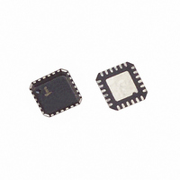
ISL6563IR Intersil, ISL6563IR Datasheet - Page 14

ISL6563IR
Manufacturer Part Number
ISL6563IR
Description
IC CNTRLR PWM 2-PH BUCK 24-QFN
Manufacturer
Intersil
Datasheet
1.ISL6563IR.pdf
(19 pages)
Specifications of ISL6563IR
Applications
Controller, Intel VRM9, VRM10, and AMD Hammer Applications
Voltage - Input
5 ~ 12 V
Number Of Outputs
1
Voltage - Output
0.8 ~ 1.85 V
Operating Temperature
-40°C ~ 85°C
Mounting Type
Surface Mount
Package / Case
24-VQFN Exposed Pad, 24-HVQFN, 24-SQFN, 24-DHVQFN
Lead Free Status / RoHS Status
Contains lead / RoHS non-compliant
Available stocks
Company
Part Number
Manufacturer
Quantity
Price
Company:
Part Number:
ISL6563IRZ
Manufacturer:
Intersil
Quantity:
300
The above equation assumes the current through the lower
MOSFET is always positive; if so, the total power dissipated
in each lower MOSFET is approximated by the summation of
P
UPPER MOSFET POWER CALCULATION
In addition to r
MOSFET losses are switching losses, due to currents
conducted through the device while the input voltage is
present as V
separate components, separating the upper-MOSFET
switching losses, the lower-MOSFET body diode reverse
recovery charge loss, and the upper MOSFET r
conduction loss.
In most typical circuits, when the upper MOSFET turns off, it
continues to conduct the inductor current until the voltage at
the phase node falls below ground. Once the lower
MOSFET begins conducting (via its body diode or
enhancement channel), the current in the upper MOSFET
falls to zero. In Equation 12, the required time for this
commutation is t
Similarly, the upper MOSFET begins conducting as soon as
it begins turning on. Assuming the inductor current is in the
positive domain, the upper MOSFET sees approximately the
input voltage applied across its drain and source terminals,
while it turns on and starts conducting the inductor current.
This transition occurs over a time t
the power loss is P
A third component involves the lower MOSFET’s reverse-
recovery charge, Q
diode conducts the full inductor current before it has fully
switched to the upper MOSFET, the upper MOSFET has to
provide the charge required to turn off the lower MOSFET’s
body diode. This charge is conducted through the upper
MOSFET across VIN, the power dissipated as a result,
P
Lastly, the conduction loss part of the upper MOSFET’s
power dissipation, P
Equation 15:
In this case, of course, r
upper MOSFET.
The total power dissipated by the upper MOSFET at full load
can be approximated as the summation of these results.
P
P
P
P
LMOS1
UMOS,3
UMOS 1 ,
UMOS 2 ,
UMOS 3 ,
UMOS 4 ,
and P
≈
≈
can be approximated using Equation 14:
=
=
V
V
V
r
IN
IN
DS
DS ON
IN
DS(ON)
⎛
⎜
⎝
⎛
⎜
⎝
LMOS2
(
. Upper MOSFET losses can be divided into
I
-------------
Q
I
-------------
1
OUT
OUT
rr
and the associated power loss is P
2
2
UMOS,2
f
RR
)
S
UMOS,4,
+
⎛
⎜
⎝
–
I
-------------
.
losses, a large portion of the upper-
. Since the lower MOSFET’s body
OUT
I
------------ -
I
------------ -
L PP
L PP
2
DS(ON)
,
2
,
2
⎞
⎟
⎠
.
⎞ t
⎟
⎠
⎞ t
⎟
⎠
2
⎛
⎜
⎝
⎛
⎜
⎝
d
14
can be calculated using
----
----
2
2
2
+
1
⎞
⎟
⎠
⎞
⎟
⎠
I
--------- -
is the ON-resistance of the
PP
12
f
f
S
S
2
2
, and the approximate
DS(ON)
UMOS,1
(EQ. 12)
(EQ. 13)
(EQ. 14)
(EQ. 15)
ISL6563
.
Since the power equations depend on MOSFET parameters,
choosing the correct MOSFETs can be an iterative process
that involves repetitively solving the loss equations for
different MOSFETs and different switching frequencies until
converging upon the best solution.
Current Sensing
The resistor connected between the ISEN and VCC pins
determines the gain in the load-line regulation and the
channel-current balance loop. Select the value for this
resistor based on the room temperature r
MOSFETs and the full-load total output current, I
Load Line Regulation Resistor
The load-line regulation resistor is labeled, R1 in Figure 1,
depends on the desired full-load droop voltage. At full load,
the current determined by R
creates the output voltage droop across R1. Thus, the load
line regulation resistor can be computed using Equation 17:
Frequency Compensation
The load-line regulated converter behaves in a similar
manner to a peak-current mode controller because the two
poles at the output filter LC resonant frequency split with the
introduction of current information into the control loop. The
final location of these poles is determined by the system
function, the gain of the current signal, and the value of the
compensation components, R
The solution to the system equations can be fairly
complicated. Fortunately, there is a simple approximation
that comes very close to an optimal solution. Treating the
system as though it were a voltage mode regulator by
compensating the LC poles and the ESR zero of the voltage
mode approximation yields a solution that is always stable
with very close to ideal transient performance.
R
R
1
ISEN
FIGURE 8. COMPENSATION CONFIGURATION FOR ISL6563
=
V
------------------------------------------------------ -
=
DROOP
r
---------------------- -
50 10
r
DS ON
R
DS ON
1
×
(
(
CIRCUIT
⋅
V
–
2 R
+
-
)
DROOP
6
)
R
⋅
⋅
⋅
2
I
FL
I
------- -
FL
ISEN
2
C
1
C
2
ISEN
2
COMP
and C
FB
is fed into the FB pin and
2
V
.
OUT
DS(ON)
of the lower
FL
June 10, 2010
.
(EQ. 16)
(EQ. 17)
FN9126.8


