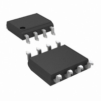
LP2996M/NOPB National Semiconductor, LP2996M/NOPB Datasheet - Page 13

LP2996M/NOPB
Manufacturer Part Number
LP2996M/NOPB
Description
IC DDR TERMINATION REG 8SOIC
Manufacturer
National Semiconductor
Datasheet
1.LP2996MNOPB.pdf
(18 pages)
Specifications of LP2996M/NOPB
Applications
Converter, DDR
Voltage - Input
2.2 ~ 5.5 V
Number Of Outputs
1
Operating Temperature
0°C ~ 125°C
Mounting Type
Surface Mount
Package / Case
8-SOIC (3.9mm Width)
Polarity
Positive
Input Voltage Max
5.5 V
Output Voltage
1.159 V, 1.259 V, 1.359 V
Output Type
Fixed
Output Current
1.5 A
Maximum Operating Temperature
+ 125 C
Mounting Style
SMD/SMT
Minimum Operating Temperature
0 C
Reference Voltage
1.358 V
Primary Input Voltage
2.5V
No. Of Outputs
1
No. Of Pins
8
Operating Temperature Range
0°C To +125°C
Msl
MSL 1 - Unlimited
Filter Terminals
SMD
Rohs Compliant
Yes
For Use With
LP2996MREVAL - BOARD EVALUATION LP2996MR
Lead Free Status / RoHS Status
Lead free / RoHS Compliant
Voltage - Output
-
Lead Free Status / Rohs Status
Details
Other names
*LP2996M
*LP2996M/NOPB
LP2996M
*LP2996M/NOPB
LP2996M
LEVEL SHIFTING
If standards other than SSTL-2 are required, such as SSTL-3,
it may be necessary to use a different scaling factor than 0.5
times V
are available to scale the output to any voltage required. One
method is to level shift the output by using feedback resistors
Conversely, the R2 resistor can be placed between V
and V
ence voltage of VDDQ/2. The equations relating VTT and the
resistors can be seen below:
HSTL APPLICATIONS
The LP2996 can be easily adapted for HSTL applications by
connecting V
DDQ
DDQ
to shift the V
for regulating the output voltage. Several options
DDQ
to the 1.5V rail. This will produce a V
TT
output lower than the internal refer-
FIGURE 11. Decreasing VTT by Level Shifting
FIGURE 10. Increasing VTT by Level Shifting
FIGURE 12. HSTL Application
TT
SENSE
and
13
from V
10 and 11. Figure 10 shows how to use two resistors to level
shift V
calculate the exact voltage at V
be used.
V
sistors. AVIN and PVIN should be connected to a 2.5V rail for
optimal performance.
REF
voltage of approximately 0.75V for the termination re-
TT
TT
to the V
above the internal reference voltage of VDDQ/2. To
SENSE
V
V
TT
TT
= VDDQ/2 ( 1 + R1/R2)
= VDDQ/2 (1 - R1/R2)
20057516
pin. This has been illustrated in Figures
20057515
20057517
TT
the following equation can
www.national.com


