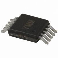
MIC2169BMM TR Micrel Inc, MIC2169BMM TR Datasheet - Page 7

MIC2169BMM TR
Manufacturer Part Number
MIC2169BMM TR
Description
IC CTRLR PWM SYNC BUCK 10-MSOP
Manufacturer
Micrel Inc
Datasheet
1.MIC2169YMM.pdf
(15 pages)
Specifications of MIC2169BMM TR
Pwm Type
Voltage Mode
Number Of Outputs
1
Frequency - Max
550kHz
Duty Cycle
92%
Voltage - Supply
3 V ~ 14.5 V
Buck
Yes
Boost
No
Flyback
No
Inverting
No
Doubler
No
Divider
No
Cuk
No
Isolated
No
Operating Temperature
-40°C ~ 85°C
Package / Case
10-MSOP, Micro10™, 10-uMAX, 10-uSOP
Frequency-max
550kHz
Lead Free Status / RoHS Status
Contains lead / RoHS non-compliant
Other names
MIC2169BMMTR
MIC2169BMMTR
MIC2169BMMTR
two hysteretic comparators that are enabled when V
within ±3% of steady state. When the output voltage reaches
97% of programmed output voltage, then the g
is enabled along with the hysteretic comparator. From this
point onwards, the voltage control loop (g
fully in control and will regulate the output voltage.
Soft-start time can be calculated approximately by adding
the following four time frames:
Current Limit
The MIC2169 uses the R
to measure output current. Since it uses the drain to source
resistance of the power MOSFET, it is not very accurate.
However, this scheme is adequate to protect the power supply
and external components during a fault condition by cutting
back the time the top MOSFET is on if the feedback voltage
is greater than 0.67V. In case of a hard short when feedback
voltage is less than 0.67V, the MIC2169 discharges the COMP
capacitor to 0.65V, resets the digital counter and automatically
shuts off the top gate drive, and the g
–3% hysteretic comparators are completely disabled and the
soft-start cycles restarts. This mode of operation is called the
“hiccup mode” and its purpose is to protect the down stream
load in case of a hard short. The circuit in Figure 1 illustrates
the MIC2169 current limiting circuit.
The current limiting resistor R
ing equation:
March 2009
Figure 1. The MIC2169 Current Limiting Circuit
t1 = Cap_COMP × 0.18V/8.5μA
t2 = 12 bit counter, approx 2ms
t3 = Cap_COMP × 0.3V/8.5μA
Soft-Start Time(Cap_COMP=100nF) = t1 + t2 + t3 +
t4 = 2.1ms + 2ms + 3.5ms + 1.8ms = 10ms
V
IN
t4
R
I
L
C2
C
IN
CS
0.1μF
=
=
200μA
I
⎛
⎜
⎝
LOAD
=
V
R
V
OUT
IN
CS
RCS
DS(ON) Q1
200 A
+
⎞
⎟ ×
⎠
2 Inductor Ripple Current
2Ω
(
μ
0.5
×
HSD
LSD
×
DS(ON)
I
L
Cap_COMP
CS
8.5 A
Q1
MOSFET N
Q2
MOSFET N
1
of the top power MOSFET
is calculated by the follow-
Equation (1)
μ
m
error amplifi er and the
1000pF
1.4Ω
m
L1 Inductor
error amplifi er) is
m
)
error amplifi er
C1
C
OUT
OUT
V
OUT
is
7
where:
200μA is the internal sink current to program the MIC2169
current limit.
The MOSFET R
therefore, it is recommended that a 50% margin be added
to the load current (I
false current limiting due to increased MOSFET junction
temperature rise. It is also recommended to connect the
R
and the R
the MOSFETs R
board layout and noise generated by the switch node. For
this a 1.4Ω resistor and a 1000pF capacitor is recommended
between the switch node and ground. A 0.1μF capacitor, in
parallel with R
switching noise.
Internal V
The MIC2169 controller internally generates V
ing and to provide power to the gate drives. This V
is generated through a low-dropout regulator and generates
5V from V
than 5V, the V
dropout. Therefore, it is recommended to short the V
to the input supply through a 5Ω resistor for input supplies
between 2.9V to 5V.
MOSFET Gate Drive
The MIC2169 high-side drive circuit is designed to switch an
N-Channel MOSFET. The block diagram on page 6 shows a
bootstrap circuit, consisting of D1 and CBST. It supplies energy
to the high-side drive circuit. Capacitor CBST is charged while
the low-side MOSFET is on and the voltage on the VSW pin
is approximately 0V. When the high-side MOSFET driver is
turned on, energy from CBST is used to turn the MOSFET
on. As the MOSFET turns on, the voltage on the VSW pin
increases to approximately V
and CBST fl oats high while continuing to keep the high-side
MOSFET on. When the low-side switch is turned back on,
CBST is recharged through D1. The drive voltage is derived
from the internal 5V V
gate drive voltage is 5V and the nominal high-side gate drive
voltage is approximately 4.5V due the voltage drop across D1.
An approximate 20ns delay between the high- and low-side
driver transition is used to prevent current from simultane-
ously fl owing unimpeded through both MOSFETs.
MOSFET Selection
The MIC2169 controller works from input voltages of 3V to
13.2V and has an internal 5V regulator to provide power to
turn the external N-Channel power MOSFETs for high- and
low-side switches. For applications where V
V
that the power MOSFETs used are sub-logic level and are in
full conduction mode for V
V
V
CS
DD
IN
OUT
> 5V; logic-level MOSFETs, whose operation is specifi ed
regulator operates in dropout mode, and it is necessary
resistor directly to the drain of the top MOSFET Q1,
Inductor Ripple Current =
F
SWITCHING
×
V
SW
IN
DD
IN
supply greater than 5V. For supply voltage less
resistor to the source of Q1 to accurately sense
×
(
Supply
DD
V
CS
F
IN
SWITCHING
DS(ON)
DS(ON)
, should be connected to fi lter some of the
linear regulator is approximately 200mV in
– V
= 500kHz
OUT
LOAD
DD
. To make the MIC2169 insensitive to
varies 30% to 40% with temperature;
)
bias supply. The nominal low-side
GS
) in the above equation to avoid
×
L
IN
of 2.5V. For applications when
. Diode D1 is reversed biased
IN
< 5V, the internal
DD
M9999-032409
for self bias-
DD
DD
supply
supply


