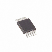
MAX1856EUB+T Maxim Integrated Products, MAX1856EUB+T Datasheet - Page 13

MAX1856EUB+T
Manufacturer Part Number
MAX1856EUB+T
Description
IC PWR SPLY PWM SLIC 10-UMAX
Manufacturer
Maxim Integrated Products
Datasheet
1.MAX1856EUB.pdf
(18 pages)
Specifications of MAX1856EUB+T
Pwm Type
Current Mode
Number Of Outputs
1
Frequency - Max
575kHz
Duty Cycle
94%
Voltage - Supply
3 V ~ 28 V
Buck
No
Boost
No
Flyback
Yes
Inverting
Yes
Doubler
No
Divider
No
Cuk
No
Isolated
No
Operating Temperature
0°C ~ 85°C
Package / Case
10-MSOP, Micro10™, 10-uMAX, 10-uSOP
Frequency-max
575kHz
Lead Free Status / RoHS Status
Lead free / RoHS Compliant
high side of R
between CS and GND.
The MAX1856 drives a wide variety of N-channel power
MOSFETs (NFETs). Since the LDO limits the EXT output
gate drive to no more than 5V, a logic-level NFET is
required. Best performance, especially with input volt-
ages below 5V, is achieved with low-threshold NFETs
that specify on-resistance with a gate-to-source voltage
(V
parameters include:
1) Total gate charge (Q
2) Reverse transfer capacitance or charge (C
3) On-resistance (R
4) Maximum drain-to-source voltage (V
5) Minimum threshold voltage (V
At high switching rates, dynamic characteristics (para-
meters 1 and 2 above) that predict switching losses
may have more impact on efficiency than R
which predicts DC losses. Q
associated with charging the gate. In addition, this
parameter helps predict the current needed to drive the
gate at the selected operating frequency. The continu-
ous LDO current for the FET gate is:
For example, the IRLL2705 has a typical Q
(at V
8.5mA.
The switching element in a flyback converter must have
a high enough voltage rating to handle the input volt-
age plus the reflected secondary voltage, as well as
any spikes induced by leakage inductance. The reflect-
ed secondary voltage is given by:
where V
diode. For a 10% variation in input voltage and a 30%
safety margin, this gives a required 33V voltage rating
(V
IRLL2705 with a V
The MAX1856’s high switching frequency demands a
high-speed rectifier. Schottky diodes are recommend-
ed for most applications because of their fast recovery
time and low forward voltage. Ensure that the diode’s
average current rating exceeds the peak secondary
GS
DS
GS
) of 2.7V or less. When selecting an NFET, key
) for the switching MOSFET in Figure 1. The
= 5V); therefore, the I
DIODE
V
REFLECT
CS
is the voltage drop across the output
I
GATE
DS
, and connect a 1000pF capacitor
______________________________________________________________________________________
DS(ON)
of 55V was chosen.
=
Power MOSFET Selection
N
N
G
=
P
S
)
Q
)
(
G
V
OUT
× ƒ
G
GATE
includes all capacitance
OSC
Wide Input Range, Synchronizable,
TH(MIN)
+
V
Diode Selection
current at 500kHz is
DIODE
DS(MAX)
)
)
G
RSS
)
of 17nC
DS(ON)
)
,
PWM SLIC Power Supply
current, using the diode manufacturer’s data or approx-
imating it with the following formula:
where N = N
ratio. Additionally, the diode’s reverse breakdown volt-
age must exceed V
plus the leakage inductance spike. For high output volt-
ages (50V or above), Schottky diodes may not be prac-
tical because of this voltage requirement. In these
cases, use a faster ultra-fast recovery diode with ade-
quate reverse-breakdown voltage.
The output capacitor (C
back converter. Typically, C
on the output ripple requirement. The output ripple is
due to the variations in the charge stored in the output
capacitor with each pulse and the voltage drop across
the capacitor’s equivalent series resistance (ESR)
caused by the current into and out of the capacitor. The
ESR-induced ripple usually dominates, so output capac-
itor selection is actually based upon the capacitor’s
ESR, voltage rating, and ripple current rating.
The input capacitor (C
the current peaks drawn from the input supply and
reduces noise injection. The value of C
determined by the source impedance of the input sup-
ply. High source impedance requires high input capac-
itance, particularly as the input voltage falls. Since
inverting flyback converters act as “constant-power”
loads to their input supply, input current rises as the
input voltage falls. Consequently, in low-input-voltage
designs, increasing C
add as much as 5% to the conversion efficiency.
In addition to C
capacitors are also required with the MAX1856. Bypass
REF to GND with 2.2µF or more. Bypass LDO to GND
with 1µF or more. And bypass V
more. All bypass capacitors should be located as close
to their respective pins as possible.
Output ripple voltage due to C
stability by introducing a left half-plane zero. A small
capacitor connected from FB to GND forms a pole with
I
D PK
(
s
/N
)
IN
P
=
I
OUT
is the secondary-to-primary turns
and C
OUT
IN
OUT
IN
plus the reflected input voltage
1
) in flyback designs reduces
and/or lowering its ESR can
OUT
+
) does all the filtering in a fly-
OUT
N V
Compensation Capacitor
V
Capacitor Selection
OUT
×
, three ceramic bypass
Output Filter Capacitor
must be chosen based
CC
Input Filter Capacitor
OUT
IN
+
Bypass Capacitors
to GND with 1µF or
ESR affects loop
∆
2
I
N
L
IN
is largely
13


