SG3525ANG ON Semiconductor, SG3525ANG Datasheet
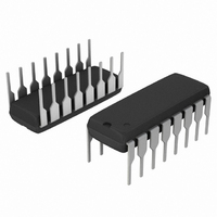
IC CTRLR PULSE WIDTH MOD 16DIP

SG3525ANG

Manufacturer Part Number
SG3525ANG
Description
IC CTRLR PULSE WIDTH MOD 16DIP
Manufacturer
ON Semiconductor
Type
Pulse Width Modulator Controllerr
Datasheets

Specifications of SG3525ANG

Pwm Type
Voltage Mode
Number Of Outputs
2
Frequency - Max
400kHz
Duty Cycle
49%
Voltage - Supply
8 V ~ 35 V
Buck
No
Boost
No
Flyback
No
Inverting
No
Doubler
No
Divider
No
Cuk
No
Isolated
No
Operating Temperature
0°C ~ 70°C
Package / Case
16-DIP (0.300", 7.62mm)
Frequency-max
400kHz
Number Of Pwm Outputs
2
On/off Pin
Yes
Adjustable Output
No
Switching Freq
400KHz
Operating Supply Voltage (max)
35V
Output Current
400A
Synchronous Pin
Yes
Rise Time
100ns
Fall Time
50ns
Operating Temperature Classification
Commercial
Mounting
Through Hole
Pin Count
16
Package Type
PDIP
Topology
Half-Bridge, Push-Pull
Switching Frequency
400 KHz
Duty Cycle (max)
49 %
Maximum Operating Temperature
+ 70 C
Minimum Operating Temperature
0 C
Mounting Style
Through Hole
Common Mode Rejection Ratio
75
Current, Input Bias
1 μA
Current, Input Offset
1 μA
Current, Output
±100 mA
Current, Supply
14 mA
Frequency, Oscillator
50 Hz to 400 kHz
Power Dissipation
1000 mW
Regulation, Line
10 mV
Regulation, Load
20 mV
Resistance, Thermal, Junction To Case
60 °C/W
Temperature, Operating, Range
0 to +70 °C
Time, Fall
50 ns
Time, Rise
100 ns
Voltage, Gain
75 dB
Voltage, Noise
40 μV
Voltage, Offset
2 mV
Voltage, Output
5.1 VDC
Voltage, Output, High
19 V
Voltage, Output, Low
0.2 V
Voltage, Supply
8 to 35 VDC
Voltage, Supply, Rejection Ratio
60 dB
Lead Free Status / RoHS Status
Lead free / RoHS Compliant
Other names
SG3525ANGOS

Available stocks

Company
Part Number
Manufacturer
Quantity
Price
Part Number:
SG3525ANG
Manufacturer:
ON Semiconductor
Quantity:
5 000
Part Number:
SG3525ANG
Manufacturer:
ST
0
Part Number:
SG3525ANG
0
Company:
Part Number:
SG3525ANG
Quantity:
20 000
Company:
Part Number:
SG3525ANG
Quantity:
5 000
SG3525A
Pulse Width Modulator
Control Circuit
improved performance and lower external parts count when
implemented for controlling all types of switching power supplies.
The on−chip +5.1 V reference is trimmed to "1% and the error
amplifier has an input common−mode voltage range that includes the
reference voltage, thus eliminating the need for external divider
resistors. A sync input to the oscillator enables multiple units to be
slaved or a single unit to be synchronized to an external system clock.
A wide range of deadtime can be programmed by a single resistor
connected between the C
features built−in soft−start circuitry, requiring only an external timing
capacitor. A shutdown pin controls both the soft−start circuitry and the
output stages, providing instantaneous turn off through the PWM latch
with pulsed shutdown, as well as soft−start recycle with longer
shutdown commands. The under voltage lockout inhibits the outputs
and the changing of the soft−start capacitor when V
nominal. The output stages are totem−pole design capable of sinking
and sourcing in excess of 200 mA. The output stage of the SG3525A
features NOR logic resulting in a low output for an off−state.
Features
*For additional information on our Pb−Free strategy and soldering details, please
January, 2005 − Rev. 5
download the ON Semiconductor Soldering and Mounting Techniques
Reference Manual, SOLDERRM/D.
The SG3525A pulse width modulator control circuit offers
8.0 V to 35 V Operation
5.1 V " 1.0% Trimmed Reference
100 Hz to 400 kHz Oscillator Range
Separate Oscillator Sync Pin
Adjustable Deadtime Control
Input Undervoltage Lockout
Latching PWM to Prevent Multiple Pulses
Pulse−by−Pulse Shutdown
Dual Source/Sink Outputs: "400 mA Peak
Pb−Free Packages are Available*
Semiconductor Components Industries, LLC, 2005
T
and Discharge pins. This device also
CC
is below
1
16
See detailed ordering and shipping information in the package
dimensions section on page 2 of this data sheet.
16
1
Noninv. Input
OSC. Output
Discharge
Soft−Start
Inv. Input
ORDERING INFORMATION
1
Sync
C
R
PIN CONNECTIONS
T
http://onsemi.com
A
WL = Wafer Lot
YY = Year
WW = Work Week
T
1
2
3
4
5
6
7
8
DW SUFFIX
CASE 751G
CASE 648
SOIC−16L
N SUFFIX
= Assembly Location
PDIP−16
(Top View)
Publication Order Number:
16
1
16
16
15
14
13
12
11
10
1
9
DIAGRAMS
V
V
Output B
V
Ground
Output A
Shutdown
Compensation
MARKING
AWLYYWW
SG3525AN
AWLYYWW
ref
CC
C
SG3525A
SG3525A/D

Related parts for SG3525ANG

SG3525ANG Summary of contents

Page 1

... Pulse−by−Pulse Shutdown Dual Source/Sink Outputs: "400 mA Peak Pb−Free Packages are Available* *For additional information on our Pb−Free strategy and soldering details, please download the ON Semiconductor Soldering and Mounting Techniques Reference Manual, SOLDERRM/D. Semiconductor Components Industries, LLC, 2005 January, 2005 − Rev. 5 http://onsemi ...

Page 2

... Noninv. Input 8 C Soft−Start 10 Shutdown ORDERING INFORMATION Device SG3525AN SG3525ANG SG3525ADW SG3525ADWG SG3525ADWR2 SG3525ADWR2G †For information on tape and reel specifications, including part orientation and tape sizes, please refer to our Tape and Reel Packaging Specifications Brochure, BRD8011/D. SG3525A To Internal Circuitry Reference Under− ...

Page 3

MAXIMUM RATINGS Rating Supply Voltage Collector Supply Voltage Logic Inputs Analog Inputs Output Current, Source or Sink Reference Output Current Oscillator Charging Current Power Dissipation T = +25 C (Note +25 C (Note 2) C Thermal ...

Page 4

ELECTRICAL CHARACTERISTICS Characteristics REFERENCE SECTION Reference Output Voltage ( Line Regulation (+8 + Load Regulation ( mA) L Temperature Stability Total Output Variation Includes Line and Load Regulation over ...

Page 5

ELECTRICAL CHARACTERISTICS Characteristics SOFT−START SECTION Soft−Start Current ( shutdown Soft−Start Voltage (V = 2.0 V) shutdown Shutdown Input Current (V = 2.5 V) shutdown OUTPUT DRIVERS (Each Output + Output Low Level (I ...

Page 6

CHARGE TIME (ms) Figure 3. Oscillator Charge Time versus R 100 ...

Page 7

Q1 5.0k Clock Output Filter + supply SG3525A 14 B GND 12 For single−ended supplies, the driver outputs are grounded. The V terminal is switched to ground by the totem−pole ...

Page 8

−T− 0.25 (0.010 SG3525A PACKAGE DIMENSIONS PDIP−16 N SUFFIX CASE 648−08 ISSUE T NOTES: 1. DIMENSIONING AND TOLERANCING PER 2. CONTROLLING DIMENSION: INCH. ...

Page 9

PACKAGE DIMENSIONS 16X 0. SEATING e PLANE 14X T SG3525A SOIC−16L DW SUFFIX CASE 751G−03 ISSUE C NOTES: 1. DIMENSIONS ARE IN MILLIMETERS INTERPRET ...

Page 10

... Fax: 480−829−7709 or 800−344−3867 Toll Free USA/Canada Email: orderlit@onsemi.com SG3525A N. American Technical Support: 800−282−9855 Toll Free USA/Canada Japan: ON Semiconductor, Japan Customer Focus Center 2−9−1 Kamimeguro, Meguro−ku, Tokyo, Japan 153−0051 Phone: 81−3−5773−3850 http://onsemi.com 10 ON Semiconductor Website: http://onsemi ...

Related keywords