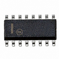
NCP1395ADR2G ON Semiconductor, NCP1395ADR2G Datasheet - Page 17

NCP1395ADR2G
Manufacturer Part Number
NCP1395ADR2G
Description
IC CTRLR PWM OVP 16SOIC
Manufacturer
ON Semiconductor
Datasheet
1.NCP1395APG.pdf
(27 pages)
Specifications of NCP1395ADR2G
Pwm Type
Voltage Mode
Number Of Outputs
1
Frequency - Max
1MHz
Duty Cycle
52%
Voltage - Supply
10.3 V ~ 20 V
Buck
No
Boost
No
Flyback
No
Inverting
No
Doubler
No
Divider
No
Cuk
No
Isolated
No
Operating Temperature
-40°C ~ 125°C
Package / Case
16-SOIC (3.9mm Width)
Frequency-max
1MHz
Switching Frequency
50 KHz to 1 MHz
Mounting Style
SMD/SMT
Duty Cycle (max)
52 %
Lead Free Status / RoHS Status
Lead free / RoHS Compliant
Other names
NCP1395ADR2G
NCP1395ADR2GOSTR
NCP1395ADR2GOSTR
Available stocks
Company
Part Number
Manufacturer
Quantity
Price
Company:
Part Number:
NCP1395ADR2G
Manufacturer:
ON Semiconductor
Quantity:
640
Company:
Part Number:
NCP1395ADR2G
Manufacturer:
ON Semiconductor
Quantity:
2 700
Part Number:
NCP1395ADR2G
Manufacturer:
ON/安森美
Quantity:
20 000
and deadtime) requires the usage of the selection charts
displayed below:
1100
900
700
500
300
100
200
180
160
140
120
100
The selection of the three setting resistors (Fmax, Fmin
Figure 38. Minimum Switching Frequency Resistor
Figure 37. Maximum switching frequency resistor
80
60
40
selection depending on the adopted minimum
20
20
70
40
switching frequency.
120
Selection
60
RFmax (kW)
RFmin (kW)
170
Fmin = 50 kHz
220
80
270
Fmin = 200 kHz
V
FB = 6.5 V
DT = 300 ns
V
FB = 1 V
DT = 300 ns
CC
CC
100
= 11 V
320
= 11 V
http://onsemi.com
370
120
17
ORing Capability
frequency variation linked to an event appearance (instead
of abruptly stopping pulses), then the FB pin lends itself
very well to the addition of other sweeping loops. Several
diodes can easily be used to perform the job in case of
reaction to a fault event or to regulate on the output current
(CC operation). Figure 40 shows how to do it.
1000
1100
900
800
700
600
500
400
300
200
100
If for a particular reason, there is a need for having a
Figure 40. Due to the FB configuration, loop ORing
0
0
Figure 39. Dead−Time Resistor Selection
V
In1
In2
CC
100
= 11 V
is easy to implement.
200
V
CC
Rdt (kW)
FB
300
20 k
400
VCO
500
600


