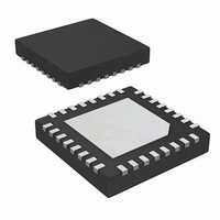
ISL9440BIRZ Intersil, ISL9440BIRZ Datasheet - Page 8

ISL9440BIRZ
Manufacturer Part Number
ISL9440BIRZ
Description
IC CTRLR PWM OUT-OF-PHASE 32-QFN
Manufacturer
Intersil
Datasheet
1.ISL9440BIRZ.pdf
(24 pages)
Specifications of ISL9440BIRZ
Pwm Type
Current Mode
Number Of Outputs
4
Frequency - Max
340kHz
Duty Cycle
93%
Voltage - Supply
4.5 V ~ 24 V
Buck
Yes
Boost
No
Flyback
No
Inverting
No
Doubler
No
Divider
No
Cuk
No
Isolated
No
Operating Temperature
-40°C ~ 85°C
Package / Case
32-VQFN Exposed Pad, 32-HVQFN, 32-SQFN, 32-DHVQFN
Frequency-max
340kHz
Lead Free Status / RoHS Status
Lead free / RoHS Compliant
Available stocks
Company
Part Number
Manufacturer
Quantity
Price
Part Number:
ISL9440BIRZ
Manufacturer:
INTERSIL
Quantity:
20 000
Company:
Part Number:
ISL9440BIRZ-T
Manufacturer:
Intersil
Quantity:
6 000
Electrical Specifications
NOTES:
10. Check Note 6 for VCC_5V and VIN configurations at 5V ±10% input applications. ISL9440B, ISL9440C’s PGOOD signal will fall LOW when VIN
11. Parameters with MIN and/or MAX limits are 100% tested at +25°C, unless otherwise specified. Temperature limits established by
PGOOD Rise Time
PGOOD Fall Time
EARLY WARNING FUNCTIONS
Undervoltage Lockout Rising (VCC_5V Pin)
Undervoltage Lockout Falling (VCC_5V Pin)
Early Warning Voltage Rising
Early Warning Voltage Falling
RST
RST Voltage Low
RST Leakage Current
RST Rise Time
RST Fall Time
PGOOD/RST TIMING RISING
VIN/VOUT Rising Threshold to PGOOD High Rising
PGOOD Rising to RST Rising
PGOOD/RST TIMING FALLING
V
PGOOD Falling to RST Falling
OVERVOLTAGE PROTECTION
OV Trip Point
OVERCURRENT PROTECTION
Overcurrent Threshold (OCSET_) (Note 8)
Full-Scale Input Current (ISEN_) (Note 8)
Overcurrent Set Voltage (OCSET_)
OVER-TEMPERATURE
Over-Temperature Shutdown
Over-Temperature Hysteresis
6. In normal operation, where the device is supplied with voltage on the V
7. This is the total shutdown current with V
8. Operating current is the supply current consumed when the device is active but not switching. It does not include gate drive current.
9. Limits established by characterization and are not production tested.
IN
/V
When the VCC_5V pin is used as a 5V supply input, the internal LDO regulator is disabled and the V
VCC_5V pin. (Refer to the“Pin Descriptions” on page 9 for more details.)
pin voltage drops below 5.55V (TYP), which results from the early warning detection on VIN pin voltage.
characterization and are not production tested.
OUT
Falling Threshold to PGOOD Falling
PARAMETER
8
Recommended operating conditions unless otherwise noted. Refer to “Block Diagram” on page 3, “Typical
Application - ISL9440B” on page 4 and “Typical Application - ISL9440C” on page 5. V
VCC_5V = 5V ±10%, C_VCC_5V = 4.7µF, T
IN
= 5.6 and 24V.
ISL9440B, ISL9440C
R
R
I_SINK = 4mA
RST = 5V
R
R
R
PULLUP
PULLUP
PULLUP
PULLUP
OCSET
IN
= 55kΩ
TEST CONDITIONS
= 10k to 3.3V
= 10k to 3.3V
= 10k to 3.3V
= 10k to 3.3V
pin, the VCC_5V pin provides a 5V output capable of 60mA (min).
A
= -40°C to +85°C, Typical values are at T
IN
input pin must be connected to the
(Note 11)
3.40
3.25
5.30
1.70
MIN
100
4.5
35
0.025
TYP
0.05
0.05
3.85
3.70
5.75
5.55
0.05
0.05
1.75
200
150
118
1.0
5.5
IN
70
32
15
20
A
= 5.6V to 24V, or
= +25°C. (Continued)
(Note 11) UNITS
MAX
4.30
4.15
5.95
1.80
300
110
0.4
6.5
1
June 24, 2010
FN6799.3
µA
ms
µA
µA
°C
°C
µs
µs
µs
µs
µs
µs
µs
%
V
V
V
V
V
V


