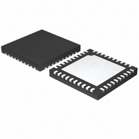
ISL6308CRZ Intersil, ISL6308CRZ Datasheet - Page 8

ISL6308CRZ
Manufacturer Part Number
ISL6308CRZ
Description
IC CTRLR PWM 3PHASE BUCK 40-QFN
Manufacturer
Intersil
Datasheet
1.ISL6308CRZ.pdf
(28 pages)
Specifications of ISL6308CRZ
Pwm Type
Voltage Mode
Number Of Outputs
1
Frequency - Max
275kHz
Duty Cycle
66.6%
Voltage - Supply
4.75 V ~ 5.25 V
Buck
Yes
Boost
No
Flyback
No
Inverting
No
Doubler
No
Divider
No
Cuk
No
Isolated
No
Operating Temperature
0°C ~ 70°C
Package / Case
40-VFQFN, 40-VFQFPN
Frequency-max
275kHz
Lead Free Status / RoHS Status
Lead free / RoHS Compliant
Available stocks
Company
Part Number
Manufacturer
Quantity
Price
Part Number:
ISL6308CRZ-T
Manufacturer:
INTERSIL
Quantity:
20 000
REF0 and REF1 (Pins 40, 39)
These pins make up the 2-bit input that selects the fixed
DAC reference voltage. These pins respond to TTL logic
thresholds. The ISL6308 decodes these inputs to establish
one of four fixed reference voltages; see Table 1 for
correspondence between REF0 and REF1 inputs and
reference voltage settings.
These pins are internally pulled high, to approximately 1.2V,
by 40µA (typically) internal current sources; the internal
pull-up current decreases to 0 as the REF0 and REF1
voltages approach the internal pull-up voltage. Both REF0
and REF1 pins are compatible with external pull-up voltages
not exceeding the IC’s bias voltage (VCC).
RGND and VSEN (Pins 10, 11)
RGND and VSEN are inputs to the precision differential
remote-sense amplifier and should be connected to the
sense pins of the remote load.
ICOMP, ISUM, and IREF (Pins 13, 15, 16)
ISUM, IREF, and ICOMP are the DCR current sense
amplifier’s negative input, positive input, and output
respectively. For accurate DCR current sensing, connect a
resistor from each channel’s phase node to ISUM and
connect IREF to the summing point of the output inductors.
A parallel R-C feedback circuit connected between ISUM
and ICOMP will then create a voltage from IREF to ICOMP
proportional to the voltage drop across the inductor DCR.
This voltage is referred to as the droop voltage and is added
to the differential remote-sense amplifier’s output.
An optional 0.001µF to 0.01µF ceramic capacitor can be
placed from the IREF pin to the ISUM pin to help reduce
common mode noise that might be introduced by the layout.
DROOP (Pin 14)
This pin enables or disables droop. Tie this pin to the ICOMP
pin to enable droop. To disable droop, tie this pin to the IREF
pin.
VDIFF (Pin 9)
VDIFF is the output of the differential remote-sense
amplifier. The voltage on this pin is equal to the difference
between VSEN and RGND added to the difference between
IREF and ICOMP. VDIFF therefore represents the VOUT
voltage plus the droop voltage.
COMP and FB (Pins 7, 8)
The internal error amplifier’s inverting input and output
respectively. FB is connected to VDIFF through an external R
or R-C network depending on the desired type of
compensation (Type II or III). COMP is tied back to FB
through an external R-C network to compensate the regulator.
8
ISL6308
DAC (Pin 3)
The DAC pin is the direct output of the internal DAC. This pin
is connected to the REF pin using a 1kΩ to 5kΩ resistor.
This pin can be left open if an external reference is used.
REF (Pin 4)
The REF input pin is the positive input of the error amplifier.
This pin can be connected to the DAC pin using a resistor
(1kΩ to 5kΩ) when the internal DAC voltage is used as the
reference voltage. When an external voltage reference is
used, it must be connected directly to the REF pin, while the
DAC pin is left unconnected. The output voltage will be
regulated to the voltage at the REF pin unless this voltage
is greater than the voltage at the DAC pin. If an external
reference is used at this pin, its magnitude cannot exceed
1.75V.
A capacitor is used between the REF pin and ground to
smooth the DAC voltage during soft-start.
OFST (Pin 5)
The OFST pin provides a means to program a DC current for
generating an offset voltage across the resistor between FB
and VDIFF. The offset current is generated via an external
resistor and precision internal voltage references. The
polarity of the offset is selected by connecting the resistor to
GND or VCC. For no offset, the OFST pin should be left
unconnected.
OCSET (Pin 12)
This is the overcurrent set pin. Placing a resistor from OCSET
to ICOMP, allows a 100µA current to flow out of this pin,
producing a voltage reference. Internal circuitry compares the
voltage at OCSET to the voltage at ISUM, and if ISUM ever
exceeds OCSET, the overcurrent protection activates.
ISEN1, ISEN2 and ISEN3 (Pins 32, 25, 19)
These pins are used for balancing the channel currents by
sensing the current through each channel’s lower MOSFET
when it is conducting. Connect a resistor between the
ISEN1, ISEN2, and ISEN3 pins and their respective phase
node. This resistor sets a current proportional to the current
in the lower MOSFET during its conduction interval.
UGATE1, UGATE2, and UGATE3 (Pins 31, 27, 20)
Connect these pins to the upper MOSFETs’ gates. These
pins are used to control the upper MOSFETs and are
monitored for shoot-through prevention purposes. Maximum
individual channel duty cycle is limited to 66%.
BOOT1, BOOT2, and BOOT3 (Pins 30, 26, 21)
These pins provide the bias voltage for the upper MOSFETs’
drives. Connect these pins to appropriately-chosen external
bootstrap capacitors. Internal bootstrap diodes connected to
the PVCC pins provide the necessary bootstrap charge.
September 30, 2008
FN9208.4


