ISL6559CRZ-T Intersil, ISL6559CRZ-T Datasheet
ISL6559CRZ-T
Specifications of ISL6559CRZ-T
Available stocks


Related parts for ISL6559CRZ-T

ISL6559CRZ-T Summary of contents
Page 1
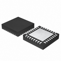
... VSEN 13 RGND 14 CAUTION: These devices are sensitive to electrostatic discharge; follow proper IC Handling Procedures. 1-888-INTERSIL or 321-724-7143 Dynamic VID is a trademark of Intersil Americas Inc. All other trademarks mentioned are the property of their respective owners. ISL6559 FN9084.8 Current Sharing DS(ON) ISL6559CR (32 LEAD QFN) TOP VIEW ...
Page 2
... PART # M28.3 ISL6559CR-T M28.3 ISL6559CRZ- 5x5 QFN Tape and Reel (Pb-free) NOTE: * Intersil Pb-free products employ special Pb-free material sets; molding compounds/die attach materials and 100% matte tin plate termination finish, which are RoHS compliant and compatible with both SnPb and Pb-free soldering operations. Intersil Pb-free products are L32 ...
Page 3
Typical Application - 3 Phase Converter 300Ω ISL6559 VSEN VCC RGND PWM4 VDIFF ISEN4 PWM1 C C IOUT ISEN1 R C COMP PWM2 OFS ISEN2 R OFS FS/DIS PWM3 R T ISEN3 VID4 VID3 VID2 VID1 VID0 ...
Page 4
Absolute Maximum Ratings Supply Voltage, VCC . . . . . . . . . . . . . . . . . . . . . . . . . . . . . . . . . +7V ...
Page 5
Electrical Specifications Operating Conditions: VCC = 5V, T PARAMETER ERROR AMPLIFIER Open-Loop Gain Open-Loop Bandwidth Slew Rate Maximum Output Voltage Source Current Sink Current REMOTE-SENSE AMPLIFIER Input Impedance Bandwidth Slew Rate SENSE CURRENT IOUT Accuracy ISEN Offset Voltage Over-Current Trip ...
Page 6
... Pull this pin below 1.14V, taking into account the enable hysteresis, to disable the controller once in operation. Connect a resistor divider to this pin to set the power-on voltage level for proper coordination with Intersil 6 ISL6559 MOSFET drivers. If this function is not required, simply tie ...
Page 7
To understand the reduction of ripple current amplitude in the multi-phase circuit, examine the equation representing an individual channel’s peak-to-peak inductor current – OUT OUT I = ----------------------------------------------------- - ...
Page 8
... The output of the error amplifier sawtooth waveform to modulate the pulse width of the PWM Σ 3 signals. The PWM signals control the timing of the Intersil I 2 MOSFET drivers and regulate the converter output to the specified reference voltage. Three distinct inputs to the error amplifier determine the voltage level of V and external circuitry which control voltage regulation is illustrated in Figure 5 ...
Page 9
... DAC) plus offset errors in the OFS current source, remote- sense and error amplifiers. Intersil specifies the guaranteed tolerance of the ISL6559 to include all variations in current TABLE 1. VOLTAGE IDENTIFICATION CODES VID3 ...
Page 10
LOAD-LINE REGULATION Microprocessor load current demands change from near no- load to full load often during operation. The ...
Page 11
... It is important that the driver ICs reach their POR level before the ISL6559 becomes enabled. The schematic in Figure 7 demonstrates sequencing the ISL6559 with the HIP660X family of Intersil MOSFET drivers which require 12V bias. Third, the frequency select\disable input (FS/DIS) will shutdown the converter when pulled to ground ...
Page 12
-------------------------------------------------- - = 560µ DELAY 1.4 VID 1 + ---------------------------------------- - – × 160 10 FB Following the delay, the soft start ramps linearly until V reaches VID. For the system described ...
Page 13
... ISL6559 to protect the microprocessor load. First, all PWM outputs are commanded low. Directing the Intersil drivers to turn on the lower MOSFETs; shunting the output to ground preventing any further increase in output voltage. The PWM outputs remain low until VDIFF falls to the programmed DAC level at which time they go into a high- impedance state ...
Page 14
Power Stages The first step in designing a multi-phase converter is to determine the number of phases. This determination depends heavily on the cost analysis which in turn depends on system constraints that differ from one design to the next. ...
Page 15
Select the values for these resistors based on the room temperature r of the lower MOSFETs; the full-load DS(ON) operating current and the number of phases according to Equation 19 (see also Figure 3). r ...
Page 16
Case 1: 0 2π LC 2π ----------------------------------- - C FB 0.75V IN ...
Page 17
In Equations 24 the per-channel filter inductance divided by the number of active channels the sum total of all output capacitors; ESR is the equivalent-series resistance of the bulk output-filter capacitance; and V the peak-to-peak sawtooth ...
Page 18
Application on page 3). Figure 15 and Equation 29 are provided to assist in the selecting the correct value for R 1000 100 10 10 100 SWITCHING FREQUENCY (kHz) FIGURE 14 SWITCHING FREQUENCY ...
Page 19
... Align the output inductors and MOSFETs such that space between the components is minimized while creating the PHASE plane. Place the Intersil HIP660X drivers as close as possible to the MOSFETs they control to reduce the parasitics due to trace length between critical driver input and output signals ...
Page 20
Small Outline Plastic Packages (SOIC) N INDEX 0.25(0.010) H AREA E - SEATING PLANE - -C- α 0.10(0.004) 0.25(0.010 NOTES: 1. Symbols are defined in the ...
Page 21
... Accordingly, the reader is cautioned to verify that data sheets are current before placing orders. Information furnished by Intersil is believed to be accurate and reliable. However, no responsibility is assumed by Intersil or its subsidiaries for its use; nor for any infringements of patents or other rights of third parties which may result from its use ...