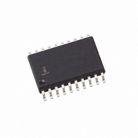
HIP6301CBZ Intersil, HIP6301CBZ Datasheet - Page 7

HIP6301CBZ
Manufacturer Part Number
HIP6301CBZ
Description
IC CONTROLLER PWM BUCK 20-SOIC
Manufacturer
Intersil
Datasheet
1.HIP6301CBZ.pdf
(17 pages)
Specifications of HIP6301CBZ
Pwm Type
Controller
Number Of Outputs
1
Frequency - Max
336kHz
Duty Cycle
75%
Voltage - Supply
4.75 V ~ 5.25 V
Buck
Yes
Boost
No
Flyback
No
Inverting
No
Doubler
No
Divider
No
Cuk
No
Isolated
No
Operating Temperature
0°C ~ 70°C
Package / Case
20-SOIC (7.5mm Width)
Frequency-max
336kHz
Lead Free Status / RoHS Status
Lead free / RoHS Compliant
Available stocks
Company
Part Number
Manufacturer
Quantity
Price
Company:
Part Number:
HIP6301CBZ
Manufacturer:
Intersil
Quantity:
310
Part Number:
HIP6301CBZ
Manufacturer:
INTERSIL
Quantity:
20 000
Electrical Specifications
Operation
Figure 1 shows a simplified diagram of the voltage regulation
and current control loops. Both voltage and current feedback
are used to precisely regulate voltage and tightly control
output currents, I
voltage loop comprises the Error Amplifier, Comparators,
gate drivers and output MOSFETs. The Error Amplifier is
essentially connected as a voltage follower that has as an
input, the Programmable Reference DAC and an output that
is the CORE voltage.
Voltage Loop
Feedback from the CORE voltage is applied via resistor R
to the inverting input of the Error Amplifier. This signal can
PROTECTION
Overvoltage Threshold
Percent Overvoltage Hysteresis
FIGURE 1. SIMPLIFIED BLOCK DIAGRAM OF THE HIP6301 VOLTAGE AND CURRENT CONTROL LOOPS FOR A TWO POWER
FB
AMPLIFIER
PROGRAMMABLE
REFERENCE
DAC
ERROR
-
+
PARAMETER
CHANNEL REGULATOR
R
IN
L1
and I
L2
CORRECTION
CORRECTION
, of the two power channels. The
+
+
-
-
7
∑
∑
∑
∑
Operating Conditions: V
-
-
I AVERAGE
+
+
VSEN Rising
VSEN Falling after Overvoltage
+
-
+
-
COMPARATOR
AVERAGING
COMPARATOR
CURRENT
HIP6303
CC
= 5V, T
CURRENT
CURRENT
SENSING
SENSING
IN
HIP6301
HIP6301
TEST CONDITIONS
CIRCUIT
CIRCUIT
A
PWM
PWM
= 0°C to 70°C, Unless Otherwise Specified (Continued)
drive the Error Amplifier output either high or low, depending
upon the CORE voltage. Low CORE voltage makes the
amplifier output move towards a higher output voltage level.
Amplifier output voltage is applied to the positive inputs of
the Comparators via the Correction summing networks. Out-
of-phase sawtooth signals are applied to the two
Comparators inverting inputs. Increasing Error Amplifier
voltage results in increased Comparator output duty cycle.
This increased duty cycle signal is passed through the PWM
CIRCUIT with no phase reversal and on to the HIP6601B,
again with no phase reversal for gate drive to the upper
MOSFETs, Q1 and Q3. Increased duty cycle or ON time for
the MOSFET transistors results in increased output voltage
to compensate for the low output voltage sensed.
PWM1
PWM2
I
I
SEN1
SEN2
HIP6601B
HIP6601B
R
R
ISEN2
ISEN1
Q2
Q4
V
V
IN
IN
Q1
Q3
PHASE
PHASE
1.12
MIN
L
I
01
-
L1
L
I
02
L2
TYP
1.15
2
V
C
CORE
December 27, 2004
MAX
OUT
1.2
-
UNITS
R
FN4765.6
V
LOAD
DAC
%


