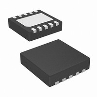
ISL6341ACRZ Intersil, ISL6341ACRZ Datasheet - Page 16

ISL6341ACRZ
Manufacturer Part Number
ISL6341ACRZ
Description
IC CTRLR SYNC BUCK PWM 10-TDFN
Manufacturer
Intersil
Datasheet
1.ISL6341CRZ.pdf
(17 pages)
Specifications of ISL6341ACRZ
Pwm Type
Voltage Mode
Number Of Outputs
1
Frequency - Max
660kHz
Duty Cycle
75%
Voltage - Supply
4.5 V ~ 14.4 V
Buck
Yes
Boost
No
Flyback
No
Inverting
No
Doubler
No
Divider
No
Cuk
No
Isolated
No
Operating Temperature
0°C ~ 70°C
Package / Case
10-TDFN Exposed Pad
Frequency-max
660kHz
Lead Free Status / RoHS Status
Lead free / RoHS Compliant
Available stocks
Company
Part Number
Manufacturer
Quantity
Price
Part Number:
ISL6341ACRZ
Manufacturer:
INTERSIL
Quantity:
20 000
For a through-hole design, several electrolytic capacitors may
be needed. For surface mount designs, solid tantalum
capacitors can also be used, but caution must be exercised
with regard to the capacitor surge current rating. These
capacitors must be capable of handling the surge current at
power-up. Some capacitor series available from reputable
manufacturers are surge current tested.
MOSFET Selection/Considerations
The ISL6341x requires 2 N-Channel power MOSFETs. These
should be selected based upon r
requirements, and thermal management requirements.
In high-current applications, the MOSFET power dissipation,
package selection and heatsink are the dominant design
factors. The power dissipation includes two loss components;
conduction loss and switching loss. The conduction losses are
the largest component of power dissipation for both the upper
and the lower MOSFETs. These losses are distributed between
the two MOSFETs according to duty factor. The switching
losses seen when sourcing current will be different from the
switching losses seen when sinking current. When sourcing
current, the upper MOSFET realizes most of the switching
losses. The lower switch realizes most of the switching losses
when the converter is sinking current (see Equation 12).
Equation 12 assumes linear voltage-current transitions and
does not adequately model power loss due to the reverse-
recovery of the upper and lower MOSFET’s body diode. The
gate-charge losses are dissipated by the ISL6341x and don't
heat the MOSFETs. However, large gate-charge increases the
switching interval, t
losses. Ensure that both MOSFETs are within their maximum
junction temperature at high ambient temperature by
calculating the temperature rise according to package
thermal-resistance specifications. A separate heatsink may be
necessary depending upon MOSFET power, package type,
ambient temperature and air flow.
When operating with a 12V power supply for V
to a minimum supply voltage of 4.5V), a wide variety of
N-MOSFETs can be used. Check the absolute maximum
V
highest V
means a 20V V
30V V
(around 1V or below) are not recommended, as explained in
the following.
Losses while Sinking Current
Losses while Sourcing Current
GS
P
P
P
P
UPPER
UPPER
LOWER
LOWER
rating for both MOSFETs; it needs to be above the
Where: D is the duty cycle = V
DS
CC
maximum rating). Low threshold transistors
= Io
= Io
=
=
t
f
voltage allowed in the system; that usually
SW
SW
Io
2
Io
2
GS
2
x r
2
x r
is the combined switch ON and OFF time, and
is the switching frequency.
×
×
SW
DS(ON)
r
DS(ON)
rating (which typically correlates with a
r
DS ON
DS ON
which increases the MOSFET switching
(
(
x D
x (1 - D)
)
)
×
×
D
16
(
1 D
+
DS(ON)
–
1
-- - Io
2
OUT
⋅
)
+
ISL6341, ISL6341A, ISL6341B, ISL6341C
/ V
×
1
-- - Io
2
, gate supply
V
⋅
IN
IN
,
×
×
V
t
SW
IN
CC
×
×
t
F
(or down
SW
S
(EQ. 12)
×
F
S
For 5V only operation, given the reduced available gate bias
voltage (5V), logic-level transistors should be used for both
N-MOSFETs. Look for r
should be exercised with devices exhibiting very low
V
present aboard the ISL6341x may be circumvented by these
MOSFETs if they have large parasitic impedences and/or
capacitances that would inhibit the gate of the MOSFET from
being discharged below its threshold level before the
complementary MOSFET is turned on. Also avoid MOSFETs
with excessive switching times; the circuitry is expecting
transitions to occur in under 50ns or so.
BOOTSTRAP Considerations
Figure 15 shows the upper gate drive (BOOT pin) supplied
by a bootstrap circuit from V
usually shares the V
in the 5V to 12V range. The boot capacitor, C
develops a floating supply voltage referenced to the PHASE
pin. The supply is refreshed to a voltage of V
boot diode drop (V
turns on. Check that the voltage rating of the capacitor is
above the maximum V
should be sufficient for a 12V system. A value of 0.1µF is
typical for many systems driving single MOSFETs.
If V
option is to connect the BOOT pin to 12V, and remove the
BOOT cap (although, you may want to add a local capacitor
from BOOT to GND). This will make the UGATE V
equal to (12V - 5V = 7V). That should be high enough to
drive most MOSFETs, and low enough to improve the
efficiency slightly. This also saves a boot diode and
capacitor.
GS(ON)
+
CC
-
VCC
ISL6341x
+V
is 12V, but V
FIGURE 15. UPPER GATE DRIVE BOOTSTRAP
CC
GND
characteristics. The shoot-through protection
VCC
D
IN
LGATE/OCSET
BOOT
UGATE
PHASE
) each time the lower MOSFET, Q
IN
CC
is lower (such as 5V), then another
or V
DS(ON)
+V
voltage in the system; a 16V rating
CC
GD
C
GD
BOOT
supply; it can be any voltage
. For convenience, V
ratings at 4.5V. Caution
+V
IN
Q1
Q2
V
V
GD
BOOT
G-S
G-S
December 2, 2008
less the
≈
≈
GS
V
V
,
GD
GD
CC
voltage
FN6538.2
2
- V
,
D


