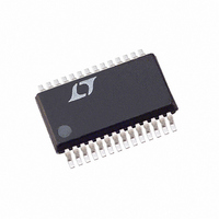
LTC1873EG#TR Linear Technology, LTC1873EG#TR Datasheet - Page 5

LTC1873EG#TR
Manufacturer Part Number
LTC1873EG#TR
Description
IC REG SW 2PH DUAL SYNC 28SSOP
Manufacturer
Linear Technology
Datasheet
1.LTC1873EG.pdf
(32 pages)
Specifications of LTC1873EG#TR
Pwm Type
Voltage Mode
Number Of Outputs
2
Frequency - Max
750kHz
Duty Cycle
93%
Voltage - Supply
3 V ~ 7 V
Buck
Yes
Boost
No
Flyback
No
Inverting
No
Doubler
No
Divider
No
Cuk
No
Isolated
No
Operating Temperature
-40°C ~ 85°C
Package / Case
28-SSOP
Frequency-max
750kHz
Lead Free Status / RoHS Status
Contains lead / RoHS non-compliant
Available stocks
Company
Part Number
Manufacturer
Quantity
Price
PI FU CTIO S
PV
power to the two BG n output drivers. PV
connected to a voltage high enough to fully turn on the
external MOSFETs QB1 and QB2. PV
be connected directly to V
bypass capacitor directly to PGND.
BOOST1 (Pin 2): Controller 1 Top Gate Driver Supply. The
BOOST1 pin supplies power to the floating TG1 driver.
BOOST1 should be bypassed to SW1 with a 1 F capacitor.
An additional Schottky diode from V
create a complete floating charge-pumped supply at
BOOST1. No other external supplies are required.
BG1 (Pin 3): Controller 1 Bottom Gate Drive. The BG1 pin
drives the gate of the bottom N-channel synchronous
switch MOSFET, QB1. BG1 is designed to drive up to
10,000pF of gate capacitance directly. If RUN/SS1 goes
low, BG1 will go low, turning off QB1. If FAULT mode is
tripped, BG1 will go high and stay high, keeping QB1 on
until the power is cycled.
TG1 (Pin 4): Controller 1 Top Gate Drive. The TG1 pin
drives the gate of the top N-channel MOSFET, QT1. The
TG1 driver draws power from the BOOST1 pin and returns
to the SW1 pin, providing true floating drive to QT1. TG1
is designed to drive up to 10,000pF of gate capacitance
directly. In shutdown or fault modes, TG1 will go low.
SW1 (Pin 5): Controller 1 Switching Node. SW1 should be
connected to the switching node of converter 1. The TG1
driver ground returns to SW1, providing floating gate
drive to the top N-channel MOSFET switch, QT1. The
voltage at SW1 is compared to I
comparator while the bottom MOSFET, QB1, is on.
I
pin sets the current limit comparator threshold for
controller 1. If the voltage drop across the bottom MOSFET,
QB1, exceeds the magnitude of the voltage at I
controller 1 will go into current limit. The I
internal 10 A current source pull-up, allowing the current
threshold to be set with a single external resistor to PGND.
This current setting resistor should be Kelvin connected to
the source of QB1. See the Current Limit Programming
section for more information on choosing R
MAX1
CC
U
(Pin 1): Driver Power Supply Input. PV
(Pin 6): Controller 1 Current Limit Set. The I
U
U
IN
. PV
CC
MAX1
requires at least a 1 F
IN
CC
by the current limit
to BOOST1 pin will
should generally
MAX1
IMAX
CC
CC
pin has an
provides
must be
.
MAX1
MAX1
,
FCB (Pin 7): Force Continuous Bar. The FCB pin forces
both converters to maintain continuous synchronous
operation regardless of load when the voltage at FCB
drops below 0.8V. FCB is normally tied to V
continuous operation, tie FCB to SGND. FCB can also be
connected to a feedback resistor divider from a secondary
winding on one converter’s inductor to generate a third
regulated output voltage. Do not leave FCB floating.
RUN/SS1 (Pin 8): Controller 1 Run/Soft-Start. Pulling
RUN/SS1 to SGND will disable controller 1 and turn off
both of its external MOSFET switches. Pulling both
RUN/SS pins down will shut down the entire LTC1873,
dropping the quiescent supply current below 50 A. A
capacitor from RUN/SS1 to SGND will control the turn-on
time and rate of rise of the controller 1 output voltage at
power-up. An internal 3.5 A current source pull-up at
RUN/SS1 pin sets the turn-on time at approximately
50ms/ F.
COMP1 (Pin 9): Controller 1 Loop Compensation. The
COMP1 pin is connected directly to the output of the first
controller’s error amplifier and the input to the PWM
comparator. An RC network is used at the COMP1 pin to
compensate the feedback loop for optimum transient
response.
SGND (Pin 10): Signal Ground. All internal low power
circuitry returns to the SGND pin. Connect to a low
impedance ground, separated from the PGND node. All
feedback, compensation and soft-start connections should
return to SGND. SGND and PGND should connect only at
a single point, near the PGND pin and the negative plate of
the C
FB1 (Pin 11): Controller 1 Feedback Input. The loop
compensation network for controller 1 should be con-
nected to FB1. FB1 is connected internally to the VID
resistor network to set the output voltage at side 1.
SENSE (Pin 12): Output Sense. Connect to V
VID0 to VID4 (Pins 13 to 17): VID Programming Inputs.
These are logic inputs that set the output voltage at side 1
to a preprogrammed value (see Table 1). VID4 is the MSB,
VID0 is the LSB. The codes selected by the VID n inputs
correspond to the Intel Desktop VID specification. Each
IN
bypass capacitor.
LTC1873
CC
OUT1
. To force
.
5


