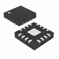
MAX8599ETE+ Maxim Integrated Products, MAX8599ETE+ Datasheet - Page 17

MAX8599ETE+
Manufacturer Part Number
MAX8599ETE+
Description
IC CNTRLR STP DWN LDO 16-TQFN
Manufacturer
Maxim Integrated Products
Datasheet
1.MAX8597ETP.pdf
(24 pages)
Specifications of MAX8599ETE+
Pwm Type
Controller
Number Of Outputs
1
Frequency - Max
1.4MHz
Duty Cycle
99.5%
Voltage - Supply
4.5 V ~ 28 V
Buck
Yes
Boost
No
Flyback
No
Inverting
No
Doubler
No
Divider
No
Cuk
No
Isolated
No
Operating Temperature
-40°C ~ 85°C
Package / Case
16-TQFN Exposed Pad
Frequency-max
1.4MHz
Lead Free Status / RoHS Status
Lead free / RoHS Compliant
I
equals twice the output voltage (V
I
mended due to their low ESR and ESL at high frequen-
cy, with relatively lower cost. Choose a capacitor that
exhibits less than 10°C temperature rise at the maximum
operating RMS current for optimum long-term reliability.
The key selection parameters for the output capacitor
are the actual capacitance value, the equivalent series
resistance (ESR), the equivalent series inductance
(ESL), and the voltage-rating requirements, which
affect the overall stability, output ripple voltage, and
transient response. The output ripple has three compo-
nents: variations in the charge stored in the output
capacitor, voltage drop across the capacitor’s ESR,
and voltage drop across the capacitor’s ESL, caused
by the current into and out of the capacitor. The follow-
ing equations estimate the worst-case ripple:
where I
The response to a load transient depends on the select-
ed output capacitor. After a load transient, the output
instantly changes by (ESR x ∆I
Before the controller can respond, the output deviates
further depending on the inductor and output capacitor
values. After a short period of time (see the Typical
Operating Characteristics), the controller responds by
regulating the output voltage back to its nominal state.
The controller response time depends on the closed-
loop bandwidth. With higher bandwidth, the response
time is faster, preventing the output capacitor voltage
from further deviation from its regulation value. Do not
exceed the capacitor’s voltage or ripple current ratings.
RMS(MAX)
RMS
I
V
V
V
V
P P
RIPPLE
RIPPLE ESR
RIPPLE ESL
RIPPLE C
−
has a maximum value when the input voltage
P-P
=
⎛
⎜
⎝
= I
is the peak-to-peak inductor current.
(
(
( )
V
=
IN
LOAD
f
S
=
V
)
−
)
RIPPLE ESR
×
=
V
=
8
OUT
______________________________________________________________________________________
L
I
V
P P
×
/ 2. Ceramic capacitors are recom-
L
IN
−
(
C
⎞
⎟ ×
⎠
+
I
×
×
P P
OUT
−
ESL
ESR
ESL
)
⎛
⎜
⎝
+
V
×
V
OUT
V
RIPPLE ESL
IN
f
S
LOAD
Output Capacitor
⎞
⎟
⎠
Low-Dropout, Wide-Input-Voltage,
IN
(
) + (ESL x di/dt).
= 2 x V
)
+
V
RIPPLE C
OUT
), so
( )
The MAX8597/MAX8598/MAX8599 controllers drive
external, logic-level, n-channel MOSFETs as the circuit-
switch elements. The key selection parameters are:
• On-resistance (R
• Maximum drain-to-source voltage (V
• Gate charges (Q
Choose MOSFETs with R
a good compromise between efficiency and cost,
choose the high-side MOSFET that has conduction loss
equal to the switching loss at the nominal input voltage
and maximum output current. For the low-side MOSFET,
make sure it does not spuriously turn on due to dv/dt
caused by the high-side MOSFET turning on, resulting in
efficiency degrading shoot-through current. MOSFETs
with a lower Q
For proper thermal-management design, the power dis-
sipation must be calculated at the desired maximum
operating junction temperature, maximum output current,
and worst-case input voltage (for low-side MOSFET,
worst case is at V
be either at V
High-side and low-side MOSFETs have different loss
components due to the circuit operation. The low-side
MOSFET operates as a zero-voltage switch; therefore,
the major losses are the channel-conduction loss
(P
where V
the dead-time between the high-side MOSFET and the
low-side MOSFET switching transitions, and f
switching frequency. The high-side MOSFET operates
as a duty-cycle control switch and has the following
major losses: the channel-conduction loss (P
V-I overlapping switching loss (P
loss (P
body-diode conduction loss because the diode never
conducts current:
Use R
where I
rent capability determined by:
Step-Down Controllers
LSCC
at least 20% higher than the input supply rail at the
high-side MOSFET’s drain.
P
P
HSSW
LSCC
DS(ON)
P
) and the body-diode conduction loss (P
HSDR
GATE
F
HSCC
is the body-diode forward-voltage drop, t
= V
= [1 - (V
P
). The high-side MOSFET does not have
IN(MIN)
LSDC
at T
is the average DH-high driver output-cur-
I
gd
GATE
IN
= (V
/Q
x I
IN(MAX)
J(MAX)
gs
OUT
= 2 x I
LOAD
g
OUT
DS(ON)
= 2.5 / (R
or V
, Q
ratio have higher immunity to dv/dt.
/ V
gd
:
IN(MAX)
/ V
; for high-side MOSFET, it could
DS(ON)
LOAD
x f
IN
, Q
): the lower, the better.
IN
S
) x I
)] x (I
gs
DH
x [(Q
x V
): the lower, the better.
).
LOAD
MOSFET Selection
rated at V
+ R
LOAD
F
HSSW
gs
x t
GATE
2
+ Q
dt
x R
DSS
)
), and the drive
2
x f
gd
)
GS
x R
DS(ON)
): should be
S
) / I
DS(ON)
= 4.5V. For
HSCC
GATE
LSDC
S
is the
), the
dt
]
):
17
is


