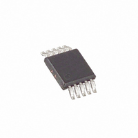
MAX1856EUB+ Maxim Integrated Products, MAX1856EUB+ Datasheet - Page 14

MAX1856EUB+
Manufacturer Part Number
MAX1856EUB+
Description
IC PS PWM SLIC SYNCH 10-UMAX
Manufacturer
Maxim Integrated Products
Datasheet
1.MAX1856EUB.pdf
(18 pages)
Specifications of MAX1856EUB+
Pwm Type
Current Mode
Number Of Outputs
1
Frequency - Max
575kHz
Duty Cycle
94%
Voltage - Supply
3 V ~ 28 V
Buck
No
Boost
No
Flyback
Yes
Inverting
Yes
Doubler
No
Divider
No
Cuk
No
Isolated
No
Operating Temperature
0°C ~ 85°C
Package / Case
10-MSOP, Micro10™, 10-uMAX, 10-uSOP
Frequency-max
575kHz
Output Voltage
0 V to - 185 V
Output Current
0.3 A
Input Voltage
3 V to 28 V
Switching Frequency
500 KHz
Mounting Style
SMD/SMT
Duty Cycle (max)
94 %
Lead Free Status / RoHS Status
Lead free / RoHS Compliant
Wide Input Range, Synchronizable,
PWM SLIC Power Supply
the feedback resistance that cancels the ESR zero. The
optimum compensation value is:
where R1 and R3 are feedback resistors (Figure 3). If
the calculated value for C
capacitance value, values from 0.5C
also provide sufficient compensation.
The MAX1856 uses a current-mode controller that
employs a current-sense resistor. Immediately after
turn-on, the MAX1856 uses a 100ns current-sense
blanking period to minimize noise sensitivity. However,
when the MOSFET turns on, the secondary inductance
and the output diode’s parasitic capacitance form a
resonant circuit that causes ringing. Reflected back
through the transformer to the primary side, these oscil-
lations appear across the current-sense resistor and
last well beyond the 100ns blanking period. As shown
in Figure 1, a series RC snubber circuit at the output
diode increases the damping factor, allowing the ring-
ing to settle quickly. Applications with dual output volt-
ages require only one snubber circuit on the higher
voltage output.
The diode’s parasitic capacitance can be estimated
using the diode’s reverse voltage rating (V
capability (I
approximation is:
For the CMR1U-02 Central Semiconductor diode used
in Figure 1, the capacitance is roughly 172pF. A value
less than this (100pF) was chosen since the output
snubber only needs to dampen the ringing, so the initial
turn-on spike that occurs during the 100ns blanking
period is still present. Larger capacitance values
require more charge, thereby increasing the power dis-
sipation.
The snubber’s time constant (t
than the 100ns blanking time. A typical RC time con-
stant of 50ns was chosen for Figure 1:
When a MOSFET with a transformer load is turned off,
the drain will fly to a high voltage as a result of the ener-
gy stored in the transformer’s leakage inductance.
14
______________________________________________________________________________________
C
FB
O
=
), and recovery time (t
C
R
1
2
DIODE
4
C
=
OUT
t
SNUB
C
=
3
(
R
I t
V
O RR
FB
RRM
1
=
×
ESR
R
50
results in a nonstandard
C
3
SNUB
ns
) /(
3
COUT
R
Snubber Design
1
+
) must be smaller
FB
R
3
)
RR
to 1.5C
RRM
). A rough
), current
FB
will
During the switch on-time, current is established in the
leakage inductance (L
rent (I
tance is:
When the switch turns off, this energy is transferred to
the MOSFET’s parasitic capacitance, causing a voltage
spike at the MOSFET’s drain. For the IRLL2705 MOS-
FET, the capacitance value (C
leakage inductance energy transfers to this capaci-
tance, the drain would fly up to:
The leakage inductance is (worst case) 1% of the pri-
mary inductance value. For a 0.27µH leakage induc-
tance and a 2.5A peak current, the voltage reaches
114V at the MOSFET’s drain, which is much higher than
the MOSFET’s rated breakdown voltage. This causes
the parasitic bipolar transistor to turn on if the dv/dt at
the drain is high enough. Note that the inductive spike
adds on to the sum of the input voltage and the reflect-
ed secondary voltage already present at the drain of
the transistor (see Power MOSFET Selection).
A series combination RC snubber (R7 and C6 in Figure
3) across the MOSFET (drain to source) reduces this
spike. The energy stored in the leakage inductance
transfers to the snubber capacitor (C6) as electrostatic
energy. Therefore, C6 must be large enough to guaran-
tee the voltage spike will not exceed the breakdown
voltage, but not so large as to result in excessive power
dissipation:
Typically, a 30% safety margin is chosen so that V
at most equal to about 70% of the MOSFET’s V
ing. For example, the V
this gives a value of 1000pF for C9. The amount of
energy stored in snubber capacitor C6 has to dis-
charge through series resistor R7 in the snubber net-
work. During turn-off, the drain voltage rises in a time
period (t
22ns for the IRLL2705. The RC time constant should
therefore equal this time. Hence:
PEAK
f
) characteristic of the MOSFET used, which is
). The energy stored in the leakage induc-
V
COSS
E
C
L
6
=
=
=
L
L I
) equal to the peak primary cur-
DSS
L I
L PEAK
L PEAK
L I
V
L PEAK
2
C
C
is 55V for the IRLL2705, so
6
DS
2
DS
2
2
) is 130pF. If all of the
2
DS
C6
rat-
is


