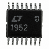
LT1952EGN#PBF Linear Technology, LT1952EGN#PBF Datasheet - Page 14

LT1952EGN#PBF
Manufacturer Part Number
LT1952EGN#PBF
Description
IC CTLR PWM SGL SWITCH 16-SSOP
Manufacturer
Linear Technology
Datasheet
1.LT1952EGNPBF.pdf
(24 pages)
Specifications of LT1952EGN#PBF
Pwm Type
Current Mode
Number Of Outputs
1
Frequency - Max
560kHz
Duty Cycle
90%
Voltage - Supply
9.25 V ~ 25 V
Buck
No
Boost
No
Flyback
Yes
Inverting
No
Doubler
No
Divider
No
Cuk
No
Isolated
Yes
Operating Temperature
-40°C ~ 125°C
Package / Case
16-SSOP
Frequency-max
560kHz
Number Of Pwm Outputs
1
On/off Pin
No
Adjustable Output
No
Topology
Flyback/Forward
Switching Freq
80 TO 560kHz
Operating Supply Voltage (max)
25V
Synchronous Pin
Yes
Rise Time
50ns
Fall Time
30ns
Operating Temperature Classification
Automotive
Mounting
Surface Mount
Pin Count
16
Package Type
SSOP N
Lead Free Status / RoHS Status
Lead free / RoHS Compliant
Available stocks
Company
Part Number
Manufacturer
Quantity
Price
APPLICATIONS INFORMATION
LT1952/LT1952-1
Blanking is provided in 2 phases (Figure 6): The fi rst phase
automatically blanks during gate rise time. Gate rise times
can vary depending on MOSFET type. For this reason the
LT1952/LT1952-1 perform true ‘leading edge blanking’ by
automatically blanking OC and I
until OUT rises to within 0.5V of V
level of 13V. The second phase of blanking starts after
the leading edge of OUT has been completed. This phase
is programmable by the user with a resistor connected
from the BLANK pin to ground. Typical durations for this
portion of the blanking period are from 45ns at R
= 10k to 540ns at R
be approximated as:
(see graph in Typical Performance Characteristics)
Programming Current Limit (OC Pin)
The LT1952/LT1952-1 use a precise 107mV sense threshold
at the OC pin to detect overcurrent conditions in the
converter and set a soft-start latch. It is independent of
duty cycle because it is not affected by slope compensation
programmed at the I
peak current in the primary MOSFET by sensing the
voltage across a sense resistor (R
14
OUT
BLANKING
Blanking (extended) = [45(R
(AUTOMATIC)
BLANKING
LEADING
0
EDGE
Figure 6. Leading Edge Blank Timing
Xns X + 45ns
R
= 10k
(MIN)
BLANK
BLANK
SENSE
10k < R
(PROGRAMMABLE)
= 120k. Blanking duration can
pin. The OC pin monitors the
EXTENDED
BLANKING
BLANK
SENSE
BLANK
IN
240k
or reaches its clamp
S
comparator outputs
/10k)]ns
[X + 45(R
) in the source of
CURRENT
BLANK
SENSE
DELAY
100ns
/10k)]ns
BLANK
1952 F06
the MOSFET. The current limit for the converter can be
programmed by:
where:
Programming Slope Compensation
The LT1952/LT1952-1 use a current mode architecture
to provide fast response to load transients and to ease
frequency compensation requirements. Current mode
switching regulators which operate with duty cycles above
50% and have continuous inductor current must add slope
compensation to their current sensing loop to prevent
subharmonic oscillations. (For more information on slope
compensation, see Application Note 19.) The LT1952/
LT1952-1 have programmable slope compensation to allow
a wide range of inductor values, to reduce susceptibility
to PCB generated noise and to optimize loop bandwidth.
The LT1952/LT1952-1 program slope compensation by
inserting a resistor R
(Figure 7). The LT1952/LT1952-1 generate a current at
the I
maximum duty cycle of the OUT pin. A simple calculation
of I(I
at the I
(See both graphs ‘I
‘I
Performance Characteristics section.)
SENSE
Current limit = (107mV/R
R
I
N
N
RIPPLE
S
S
P
SENSE
SENSE
= sense resistor in source of primary MOSFET
= number of transformer secondary turns
= number of transformer primary turns
LT1952-1
SENSE
LT1952/
CURRENT SLOPE = 35μA • DC
Maximum Threshold vs Duty Cycle’ in the Typical
Figure 7. Programming Slope Compensation
I
SENSE
= p-p ripple current in the output inductor L1
) • R
pin which is linear from 0% duty cycle to the
OUT
1952 F07
OC
pin for programmable slope compensation.
SLOPE
R
SLOPE
SENSE
gives an added ramp to the voltage
SLOPE
V
R
Pin Current vs. Duty Cycle’ and
S
S
in series with the I
S
V
I
DC = DUTY CYCLE
FOR SYNC OPERATION
I
k = f
SENSE
SENSE(SYNC)
)(N
(ISENSE)
OSC
P
= 8μA + 35DC μA
/N
/f
SYNC
= V
S
S
) – (1/2)(I
= 8μA + (k • 35DC)μA
+ (I
SENSE
• R
SLOPE
SENSE
RIPPLE
)
19521fd
)
pin


