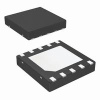
LM5033SD/NOPB National Semiconductor, LM5033SD/NOPB Datasheet - Page 5

LM5033SD/NOPB
Manufacturer Part Number
LM5033SD/NOPB
Description
IC CTRLR PWM PUSH PULL HV 10LLP
Manufacturer
National Semiconductor
Series
PowerWise®r
Datasheet
1.LM5033MMNOPB.pdf
(17 pages)
Specifications of LM5033SD/NOPB
Pwm Type
Voltage Mode
Number Of Outputs
2
Frequency - Max
1MHz
Duty Cycle
95.5%
Voltage - Supply
15 V ~ 90 V
Buck
Yes
Boost
Yes
Flyback
No
Inverting
Yes
Doubler
No
Divider
No
Cuk
No
Isolated
No
Operating Temperature
-40°C ~ 125°C
Package / Case
10-LLP
Frequency-max
1MHz
For Use With
LM5033SD-EVAL - BOARD EVALUATION LM5033SD
Lead Free Status / RoHS Status
Lead free / RoHS Compliant
Other names
LM5033SD
LM5033SDTR
LM5033SDTR
Available stocks
Company
Part Number
Manufacturer
Quantity
Price
Oscillator (Pin 9)
Fs1
Fs2
Vsync
PWM Comparator Input (Pin 3)
t
Output Drivers (Pin 5, 6)
Thermal Shutdown
T
Thermal Resistance
θ
PWM
Electrical Characteristics
Symbol
JA
Specifications with standard typeface are for T
Temperature range. V
5).
SD
Note 1: Absolute Maximum Ratings are limits beyond which damage to the device may occur. Operating Ratings are conditions under which operation of the device
is intended to be functional. For guaranteed specifications and test conditions, see the Electrical Characteristics.
Note 2: The maximum allowable power dissipation is a function of the maximum allowed junction temperature (T
junction-to-ambient thermal resistance (θ
will cause the thermal shutdown to activate.
Note 3: The human body model is a 100 pF capacitor discharged through a 1.5kΩ resistor into each pin.
Note 4: Min and Max limits are 100% production tested at 25˚C. Limits over the operating temperature range are guaranteed through correlation using Statistical
Quality Control (SQC) methods. Limits are used to calculate National’s Average Outgoing Quality Level (AOQL).
Note 5: Typical specifications represent the most likely parametric norm at 25˚C operation.
Parameter
Internal frequency
Internal frequency
Sync threshold
R
Gain from pin 3 to
PWM comparator
Maximum duty cycle at
Out1, Out2
Minimum duty cycle at
Out1, Out2
Open Circuit Voltage
Short circuit current
Deadtime (T
Rise Time
Fall Time
Output High Voltage
Output Low Voltage
Max. source current
Max. sink current
Shutdown temperature
Shutdown temperature
hysteresis
Junction to Ambient
t
/Sync DC voltage
IN
D
)
= 48V, V
JA
). The maximum allowable power dissipation can be calculated from PD = (T
CC
Rt = 26.7 kΩ
Rt = 8.2 kΩ
See PWM Comparator
text
Pin 3 = 0V.
Pin 3 = 0V
CLoad = 0
OUT2. Time measured
from 10% of falling
output to 10% of rising
output.
C
C
Iout = 50 mA (source)
Iout = 100 mA (sink)
MUB10A Package
SDC10A Package
= 10V applied externally, R
Load
Load
(Continued)
= 1nF
= 1nF
Conditions
J
= 25˚C, and those with boldface type apply over full Operating Junction
@
OUT1,
5
T
= 26.7kΩ, unless otherwise stated. See (Note 4) and (Note
Vcc-0.75
Min
175
4.2
0.6
85
(0.5T
Vcc-0.25
100 x
0.34
0.25
Typ
200
600
135
165
200
3.2
2.0
S
5.2
1.1
1.5
1.5
16
16
15
38
-T
J(max)
J(max)
D
)/T
), the ambient temperature (T
S
- T
A
) / θ
JA
. Excessive power dissipation
Max
0.75
225
185
3.8
6.2
1.5
0
www.national.com
A
), and the
Units
˚C/W
kHz
kHz
V/V
mA
ns
ns
ns
˚C
˚C
%
%
V
V
V
V
V
A
A


