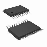
LM5034MTC/NOPB National Semiconductor, LM5034MTC/NOPB Datasheet - Page 21

LM5034MTC/NOPB
Manufacturer Part Number
LM5034MTC/NOPB
Description
IC CTRLR PWM DUAL CMODE 20TSSOP
Manufacturer
National Semiconductor
Series
PowerWise®r
Datasheet
1.LM5034MTCNOPB.pdf
(29 pages)
Specifications of LM5034MTC/NOPB
Pwm Type
Current Mode
Number Of Outputs
2
Frequency - Max
1MHz
Duty Cycle
94%
Voltage - Supply
13 V ~ 100 V
Buck
Yes
Boost
Yes
Flyback
No
Inverting
Yes
Doubler
No
Divider
No
Cuk
No
Isolated
Yes
Operating Temperature
-40°C ~ 125°C
Package / Case
20-TSSOP
Frequency-max
2MHz
For Use With
LM5034EVAL - BOARD EVALUATION LM5034
Lead Free Status / RoHS Status
Lead free / RoHS Compliant
Other names
*LM5034MTC
LM5034MTC
LM5034MTC
Applications Information
VCC1, VCC2
The capacitors at each VCC pin provide not only regulator
noise filtering and stability, but also prevents VCC from
dropping to the lower under-voltage threshold level (UVT =
6.2V) when the output drivers source current surges to the
external MOSFET gates. Additionally, the capacitors provide
a necessary time delay during startup. The time delay allows
the internal circuitry of the LM5034 and associated external
circuitry to stabilize before V
threshold level (7.6V), at which time the outputs are enabled
and the soft-start sequence begins. V
lated at 7.7V. The delay to the UVT level (Figure 3) is
calculated from the following:
where C1 and C2 are the capacitors at VCC1 and VCC2,
and I
tors are 0.1 µF each, the nominal I
a delay of approximately 69 µs. The V
should range between 0.1 µF and 25 µF, and they should be
the same value. Experimentation with the final design may
be necessary to determine the optimum value for the V
capacitors.
The average V
external MOSFETs is a function of the MOSFET gate capaci-
tance and the switching frequency (see Figure 6). To ensure
VCC does not droop below the lower UVT threshold, an
external supply should be diode connected to both VCC pins
to provide the required current, as shown in Figure 29. The
applied V
the V
external supply shuts off the internal regulator, reducing
power dissipation within the IC. Internally there is a diode
from the V
voltage is derived from an auxiliary winding on the power
transformer, or on the output inductor.
CC(Lim)
CC
voltage higher than the 7.7V regulation level with an
CC
CC
is the V
voltage must be between 8V and 15V. Providing
FIGURE 28. Shutdown Control
regulator output to VIN. Typically the applied
CC
CC
regulator current required to drive the
regulator’s current limit. If the capaci-
CC
CC(Lim)
reaches the upper UVT
CC
CC
of 22 mA provides
is nominally regu-
capacitor values
(Continued)
20136829
CC
21
OSCILLATOR, SYNC INPUT
The oscillator frequency is generally selected in conjunction
with the system magnetic components, and any other as-
pects of the system which may be affected by the frequency.
The R
according to Equation 1. Each output (OUT1 and OUT2)
switches at one-half the oscillator frequency. If the required
frequency tolerance is critical in a particular application, the
tolerance of the external resistor and the frequency toler-
ance specified in the Electrical Characteristics table must be
considered when selecting the R
If the LM5034 is to be synchronized to an external clock, that
signal must be coupled into the RT/SYNC pin through a 100
pF capacitor. The external synchronizing frequency must be
at least 4% higher than the free running frequency set by the
R
quency. The RT/SYNC pin voltage is nominally regulated at
2.0V and the external pulse amplitude should lift the pin to
between 3.8V and 5.0V on the low-to-high transition. The
synchronization pulse width should be between 15 and 150
ns. The R
is free running or externally synchronized.
VOLTAGE FEEDBACK, COMP1, COMP2
Each COMP pin is designed to accept a voltage feedback
signal from the respective regulated output via an error
amplifier and (typically) an opto-coupler. A typical configura-
tion is shown in Figure 19. V
by the error amplifier which has an appropriate frequency
compensation network. The amplifier’s output drives the
opto-coupler, which in turn drives the COMP pin.
When the LM5034’s two controller channels are configured
to provide a single high current output, COMP1 and COMP2
are typically connected together, and to the feedback signal
from the optocoupler.
CURRENT SENSE, CS1, CS2
Each CS pin receives an input signal representative of its
transformer’s primary current, either from a current sense
transformer or from a resistor in series with the source of the
primary switch, as shown in Figure 30 and Figure 31. In both
cases the sensed current creates a ramping voltage across
R1, and the R
R1, R
as possible, and the ground connection from the current
sense transformer, or R1, should be a dedicated track to the
appropriate GND pin. The current sense components must
provide
exists.
T
resistor and no higher than twice the free running fre-
F
T
and C
>
resistor at the RT/SYNC pin sets the frequency
T
0.5V at the CS pin when an over-current condition
FIGURE 29. External Power to V
resistor is always required, whether the oscillator
F
F
should be as physically close to the LM5034
/C
F
filter suppresses noise and transients.
OUT
is compared to a reference
T
resistor.
CC
www.national.com
20136830


