LM25115MT/NOPB National Semiconductor, LM25115MT/NOPB Datasheet - Page 14
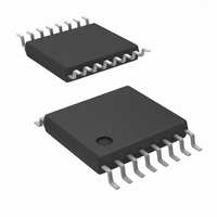
LM25115MT/NOPB
Manufacturer Part Number
LM25115MT/NOPB
Description
IC CTRLR SSPR 42V LD REG 16TSSOP
Manufacturer
National Semiconductor
Datasheet
1.LM25115SDNOPB.pdf
(17 pages)
Specifications of LM25115MT/NOPB
Pwm Type
Voltage/Current Mode
Number Of Outputs
2
Frequency - Max
1MHz
Duty Cycle
90%
Voltage - Supply
5 V ~ 7.5 V
Buck
Yes
Boost
No
Flyback
No
Inverting
No
Doubler
No
Divider
No
Cuk
No
Isolated
No
Operating Temperature
-40°C ~ 125°C
Package / Case
16-TSSOP
Frequency-max
1MHz
Lead Free Status / RoHS Status
Lead free / RoHS Compliant
Other names
*LM25115MT
*LM25115MT/NOPB
LM25115MT
*LM25115MT/NOPB
LM25115MT


www.national.com
Gate Drivers Outputs (HO & LO)
mize voltage transients due to parasitic inductances and the
high peak output currents of the drivers. The recommended
range of the HB capacitor is 0.047µF to 0.22µF.
Both drivers are controlled by the PWM logic signal from the
PWM latch. When the phase signal is low, the outputs are
held in the reset state with the low-side MOSFET on and the
high-side MOSFET off. When the phase signal switches to
the high state, the PWM latch reset signal is de-asserted.
The high-side MOSFET remains off until the PWM latch is
set by the PWM comparator (CRMIX
Figure 4). When the PWM latch is set, the LO driver turns off
the low-side MOSFET and the HO driver turns on the high-
side MOSFET. The high-side pulse is terminated when the
phase signal falls and the SYNC input comparator resets the
PWM latch.
Free-Run Mode
The LM25115 can be operated as a conventional synchro-
nous buck controller with a dc input supply instead of the
square wave phase signal. In the dc or free-run mode, the
LM25115 PWM controller synchronizes to an internal clock
signal instead of the phase signal pulses. The clock fre-
quency in the free-run mode is programmed by the SYNC
pin resistor and RAMP pin capacitor. Connecting a resistor
between a dc bias supply and the SYNC pin produces a
current I
RAMP pin capacitor . The RAMP capacitor is charged until
its voltage reaches the free-run mode peak threshold of
2.25V. The RAMP capacitor is then discharged for 300ns
(Continued)
SYNC
which controls the charging current of the
>
CV as shown in
14
before beginning a new PWM cycle. The 300ns reset time of
the RAMP pin sets the minimum off time of the PWM con-
troller in the free-run mode. The internal clock frequency in
the free-run mode is set by the synchronization current,
ramp capacitor, free-run peak threshold, and 300ns dead-
time.
Note that the VCC supply can be used as the dc bias to
produce I
longer functional in this operating mode, so the loop gain will
vary as a function of Vin. The LM25115 controls the buck
power stage with leading edge pulse width modulaton to
hold off the high-side driver until the necessary volt*seconds
is established for regulation. Other features described for the
secondary side post regulator apply in the free run mode
operation. They include voltage mode control with current
injection, positive and negative current limit, programmable
soft-start, adaptive delays for outputs, and thermal protec-
tion.
Thermal Protection
Internal thermal shutdown circuitry is provided to protect the
integrated circuit in the event the maximum junction tem-
perature limit is exceeded. When activated, typically at 165
degrees Celsius, the controller is forced into a low power
standby state with the output drivers and the bias regulator
disabled. The device will restart when the junction tempera-
ture falls below the thermal shutdown hysteresis, which is
typically 25 degrees. The thermal protection feature is pro-
vided to prevent catastrophic failures from accidental device
overheating.
F
CLK
SYNC
) 1 / ((C
. Note that the input voltage feedforward is no
RAMP
x 2.25V) / (I
SYNC
x 3) + 300ns)
Related parts for LM25115MT/NOPB
Image
Part Number
Description
Manufacturer
Datasheet
Request
R

Part Number:
Description:
IC,Multiple Regulator Circuit,TSSOP,16PIN,PLASTIC
Manufacturer:
National Semiconductor
Part Number:
Description:
National Semiconductor [8-Bit D/A Converter]
Manufacturer:
National Semiconductor
Datasheet:
Part Number:
Description:
National Semiconductor [Media Coprocessor]
Manufacturer:
National Semiconductor
Datasheet:
Part Number:
Description:
Digitally Controlled Tone and Volume Circuit with Stereo Audio Power Amplifier, Microphone Preamp Stage and National 3D Sound
Manufacturer:
National Semiconductor
Datasheet:
Part Number:
Description:
Digitally Controlled Tone and Volume Circuit with Stereo Audio Power Amplifier, Microphone Preamp Stage and National 3D Sound
Manufacturer:
National Semiconductor
Datasheet:
Part Number:
Description:
AC97 Rev 2 Codec with Sample Rate Conversion and National 3D Sound
Manufacturer:
National Semiconductor
Part Number:
Description:
Manufacturer:
National Semiconductor
Datasheet:
Part Number:
Description:
Manufacturer:
National Semiconductor
Datasheet:
Part Number:
Description:
General Purpose, Low Voltage, Low Power, Rail-to-Rail Output Operational Amplifiers
Manufacturer:
National Semiconductor
Datasheet:
Part Number:
Description:
8-bit 20 MSPS flash A/D converter.
Manufacturer:
National Semiconductor
Datasheet:
Part Number:
Description:
Low Noise Quad Operational Amplifier
Manufacturer:
National Semiconductor
Datasheet:
Part Number:
Description:
Quad Differential Line Receivers
Manufacturer:
National Semiconductor
Datasheet:
Part Number:
Description:
Quad High Speed Trapezoidal? Bus Transceiver
Manufacturer:
National Semiconductor
Datasheet:
Part Number:
Description:
Dual Line Receiver
Manufacturer:
National Semiconductor
Datasheet: