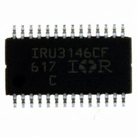
IRU3146CFTR International Rectifier, IRU3146CFTR Datasheet - Page 4

IRU3146CFTR
Manufacturer Part Number
IRU3146CFTR
Description
IC PWM DUAL SYNC 28-TSSOP
Manufacturer
International Rectifier
Specifications of IRU3146CFTR
Pwm Type
Voltage Mode
Number Of Outputs
2
Frequency - Max
345kHz
Duty Cycle
85%
Voltage - Supply
4.5 V ~ 16 V
Buck
Yes
Boost
No
Flyback
No
Inverting
No
Doubler
No
Divider
No
Cuk
No
Isolated
No
Operating Temperature
0°C ~ 70°C
Package / Case
28-TSSOP
Frequency-max
345kHz
Lead Free Status / RoHS Status
Contains lead / RoHS non-compliant
IRU3146
DEADBAND TIME
PIN DESCRIPTIONS
PIN#
4
10,18
12,16
13,15
11,17
5,23
6,22
7,21
9,19
20
14
24
25
1
2
3
4
8
OCSet2,OCSet1
Comp2, Comp1
PGnd2, PGnd1
PIN SYMBOL
HDrv2, HDrv1
VcH2, VcH1
LDrv2, LDrv1
High Side
Driver HD
V
Low Side
Driver LD
SS2 / SD
SS1 / SD
SEN2
Fb2,Fb1
PGood
Hiccup
V
Sync
Vcc
V
Rt
OUT3
, V
CL
SEN1
10%
90%
10%
90%
2V
2V
Power Good pin. Low when any of the outputs fall 10% below the set voltages.
Supply voltage for the internal blocks of the IC.
Output of the internal LDO.
Switching frequency setting resistor. (see Figure 10 for selecting resistor values).
Sense pins for OVP and PGood. For 2-Phase operation tie these pins together.
Inverting inputs to the error amplifiers. In current sharing mode, Fb1 is connected to a
resistor divider to set the output voltage and Fb2 is connected to programming resistor to
achieve current sharing. In independent 2-channel mode, these pins work as feedback
inputs for each channel.
Compensation pins for the error amplifiers.
These pins provide soft-start for the switching regulator. An internal current source charges
external capacitors that are connected from these pins to ground which ramp up the
output of the switching regulators, preventing them from overshooting as well as limiting
the input current. The converter can be shutdown by pulling these pins below 0.3V.
Current limit resistor (R
connected to the corresponding switching nodes.
Supply voltage for the high side output drivers. These are connected to voltages that must
be typically 6V higher than their bus voltages. A 1µF high frequency capacitor must be
connected from these pins to GND to provide peak drive current capability.
Output drivers for the high side power MOSFETs. 1)
These pins serve as the separate grounds for MOSFET drivers and should be connected
to the system’s ground plane.
Output drivers for the synchronous power MOSFETs.
Supply voltage for the low side output drivers. This pin should be high for normal operation
The internal oscillator may be synchronized to an external clock via this pin.
When pulled High, it puts the device current limit into a hiccup mode. When pulled Low,
the output latches off, after an overcurrent event.
PIN DESCRIPTION
Deadband
Tr
H_to_L
Figure 2 - Deadband time definition.
T
DB(TYP)
Tf
LIM
=(Deadband H_toL+Deadband L_to -H)/2
) connection pins for output 1 and 2. The other ends of R
www.irf.com
Tr
Tf
Deadband
L_to_H
Rev. 1.1
LIM
6/25/04
s are


