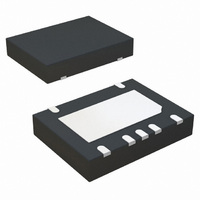
IR3629AMTRPBF International Rectifier, IR3629AMTRPBF Datasheet - Page 17

IR3629AMTRPBF
Manufacturer Part Number
IR3629AMTRPBF
Description
IC CTLR PWM SYNC BUCK 12-MLPD
Manufacturer
International Rectifier
Datasheet
1.IR3629AMTRPBF.pdf
(23 pages)
Specifications of IR3629AMTRPBF
Pwm Type
Voltage Mode
Number Of Outputs
1
Frequency - Max
330kHz
Duty Cycle
78%
Voltage - Supply
4.5 V ~ 14 V
Buck
Yes
Boost
No
Flyback
No
Inverting
No
Doubler
No
Divider
No
Cuk
No
Isolated
No
Operating Temperature
-40°C ~ 125°C
Package / Case
12-MLPD
Frequency-max
330kHz
Package
12-Lead MLPD
Circuit
Sync PWM Controller
Vcc (min)
4.0
Vcc (max)
30
Switch Freq (khz)
Internal 300kHz
Pbf
PbF Option Available
Lead Free Status / RoHS Status
Lead free / RoHS Compliant
Other names
IR3629AMTRPBFTR
Programming the Current-Limit
The Current-Limit threshold can be set by
connecting a resistor (R
low-side MOSFET to the OCSet pin. The
resistor can be calculated by using equation (3).
The
coefficient and it should be considered for the
worst case operation. This resistor must be
placed close to the IC, place a small ceramic
capacitor from this pin to ground for noise
rejection purposes.
Setting the Power Good Threshold
Power Good threshold can be programmed by
using two external resistors (R1, R2 in figure 16).
The following formulas can be used to set the
threshold:
Where;
0.38V is reference of the internal comparator
0.9*Vout is selectable threshold for power good,
for this design it is 1.62V.
Select R
Using (18): R
Select R
Use a pull up resistor (4.99K) from PGood pin to
Vcc.
11/29/2007
R
DS(on)
1
2
I
(50%
R
SET
R
I
=10KOhm
=3.09K
R
SET
DS
OCSet
2
=
(
=
on
≅
2
I
)
over
0
=3.06KOhm
( L
I
=
.
=
9
critical
o
has
(
. 3
*V
1
LIM
3 .
65
0
out
)
nominal
m
.
)
38
=
K
=
Ω
−
Ω
V
R
25
a
0
1 *
OCSet
.
SET
38
R
A
5 .
Select
DS
V
1 *
positive
=
output
) from the drain of the
∗
(
*R
on
5 .
I
. 1
OCSet
)
95
1
=
37
m
R
current)
7
Ω
5 .
--(
=
A
. 3
18
--(
temperature
65
3
)
)
K
Ω
Layout Consideration
The layout is very important when designing high
frequency switching converters. Poor layout will
affect noise pickup and can cause a good design
to perform with less than expected results.
Start to place the power components, making all
the connection in the top layer with wide, copper
filled areas. The inductor, output capacitors and
the MOSFETS should be as close to each other
as possible. This helps to reduce the EMI
radiated by the power traces due to the high
switching currents through them. Place input
capacitor very close to the drain of the high-side
MOSFET, to reduce the ESR replace the single
input capacitor with two parallel units.
The feedback part of the system should be kept
away from the inductor and other noise sources.
The
capacitors for Vcc and Vc should be close to the
respective pins. It is important to place the
feedback
resistors and compensation components close to
Fb and Comp pins.
In a multilayer PCB use one layer as a power
ground plane and have a control circuit ground
(analog ground), to which all signals are
referenced. The goal is to localize the high
current path to a separate loop that does not
interfere with the more sensitive analog control
function. These two grounds must be connected
together on the PC board layout at a single point.
The MLPD is a thermally enhanced package.
Based
recommended
effectively remove heat from the device the
exposed pad should be connected to ground
plane using vias.
critical
on
IR3629/IR3629A MPbF
components
bypass
thermal
to
use
components
performance
including
4-layers
PCB.
such
feedback
it
To
as
is
17


