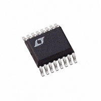
LT3150CGN Linear Technology, LT3150CGN Datasheet - Page 11

LT3150CGN
Manufacturer Part Number
LT3150CGN
Description
IC CTRLR REG VLDO FET 16-SSOP
Manufacturer
Linear Technology
Type
Positive Adjustabler
Datasheet
1.LT3150CGNPBF.pdf
(20 pages)
Specifications of LT3150CGN
Number Of Outputs
1
Voltage - Output
2.5 ~ 18.4 V
Current - Supply
12mA
Voltage - Input
1.5 ~ 10 V, 10 ~ 20 V
Operating Temperature
0°C ~ 70°C
Package / Case
16-SSOP
Lead Free Status / RoHS Status
Contains lead / RoHS non-compliant
Available stocks
Company
Part Number
Manufacturer
Quantity
Price
Company:
Part Number:
LT3150CGN
Manufacturer:
LT
Quantity:
10 000
Part Number:
LT3150CGN
Manufacturer:
LINEAR/凌特
Quantity:
20 000
Part Number:
LT3150CGN#PBF
Manufacturer:
LINEAR/凌特
Quantity:
20 000
Company:
Part Number:
LT3150CGN#TRPBF
Manufacturer:
MURATA
Quantity:
9 800
Part Number:
LT3150CGN#TRPBF
Manufacturer:
LINEAR/凌特
Quantity:
20 000
APPLICATIO S I FOR ATIO
solutions for microprocessor power supplies. This signifi-
cant performance benefit is what permits the elimination
of all bulk output capacitance.
Several other unique features are included in the design
that increase its functionality and robustness. These func-
tions comprise the remainder of the Block Diagram.
A high side sense, current limit amplifier provides active
current limiting for the regulator. The current limit ampli-
fier uses an external low value shunt resistor connected in
series with the external MOSFET’s drain. This resistor can
be a discrete shunt resistor or can be manufactured from
a Kelvin-sensed section of “free” PC board trace. All load
current flows through the MOSFET drain and thus, through
the sense resistor. The advantage of using high side
current sensing in this topology is that the MOSFET’s gain
and the main feedback loop’s gain remain unaffected. The
sense resistor develops a voltage equal to I
The current limit amplifier’s 50mV threshold voltage is a
good compromise between power dissipation in the sense
resistor, dropout voltage impact and noise immunity.
Current limit activates when the sense resistor voltage
equals the 50mV threshold.
Two events occur when current limit activates: the first is
that the current limit amplifier drives Q5 in the Block
Diagram and clamps the positive swing of the COMP node
in the main error amplifier to a voltage that provides an
output load current of 50mV/R
ues as long as the output current overload persists. The
second event is that a timer circuit activates at the SHDN2
pin. This pin is normally held low by a 5 A active pull-down
that limits to 100mV above ground. When current limit
activates, the 5 A pull-down turns off and a 15 A pull-up
current source turns on. Placing a capacitor in series with
the SHDN2 pin to ground generates a programmable time
ramp voltage.
The SHDN2 pin is also the positive input of COMP1. The
negative input is tied to the internal 1.21V reference.
When the SHDN2 pin ramps above V
drives Q7 and Q8. This action pulls the COMP and GATE
pins low and latches the external MOSFET drive off. This
condition reduces the MOSFET power dissipation to zero.
The time period until the latched-off condition occurs is
typically equal to C
U
SHDN2
U
(1.11V)/15 A. For example, a
SENSE
W
. This action contin-
REF
, the comparator
OUT
U
(R
SENSE
).
1 F capacitor on the SHDN2 pin yields a 74ms ramp time.
In short, this unique circuit block performs a current limit
time-out function that latches off the regulator drive after
a predefined time period. The time-out period selected is
a function of system requirements including start-up and
safe operating area. The SHDN2 pin is internally clamped
to typically 1.85V by Q9 and R10. The comparator tied to
the SHDN2 pin has 100mV of typical hysteresis to provide
noise immunity. The hysteresis is especially useful when
using the SHDN2 pin for thermal shutdown.
Restoring normal operation after the load current fault is
cleared is accomplished in two ways. One option is to
recycle the V
external bleed path for the SHDN2 pin capacitor is pro-
vided. The second option is to provide an active reset
circuit that pulls the SHDN2 pin below V
SHDN2 pin below V
source and reactivates the 5 A pull-down. If the SHDN2
pin is held below V
lator continues to operate in current limit into a short. This
action requires being able to sink 15 A from the SHDN2
pin at less than 1V. The 5 A pull-down current source and
the 15 A pull-up current source are designed low enough
in value so that an external resistor divider network can
drive the SHDN2 pin to provide overvoltage protection or
to provide thermal shutdown with the use of a thermistor
in the divider network. Diode-ORing these functions to-
gether is simple to accomplish and provides multiple
functionality for one pin.
If the current limit amplifier is not used, two choices
present themselves. The simplest choice is to tie the I
pin directly to the I
and provides the simplest, no frills circuit. Applications in
which the current limit amplifier is not used are where
extremely low dropout voltages must be achieved and the
50mV threshold voltage cannot be tolerated.
However, a second available choice permits a user to pro-
vide short-circuit protection with no external sensing. This
technique is activated by grounding the I
disables the current limit amplifier because Schottky diode
D1 clamps the amplifier’s output and prevents Q5 from
pulling down the COMP node. In addition, Schottky diode
D2 turns off pull-down transistor Q4. Q4 is normally on and
IN2
LT3150 supply voltage as long as an
POS
REF
REF
pin. This action defeats current limit
during a fault condition, the regu-
turns off the 15 A pull-up current
NEG
REF
pin. This action
LT3150
. Pulling the
11
NEG
3150f


