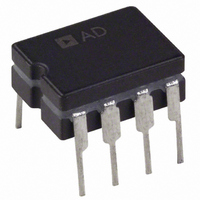
REF02EZ Analog Devices Inc, REF02EZ Datasheet - Page 12

REF02EZ
Manufacturer Part Number
REF02EZ
Description
IC VOLT REFERENCE PREC 5V 8CDIP
Manufacturer
Analog Devices Inc
Specifications of REF02EZ
Temperature Coefficient
8.5ppm/°C
Reference Type
Series
Voltage - Output
5V
Tolerance
±0.02%
Voltage - Input
7 ~ 40 V
Number Of Channels
1
Current - Quiescent
1.4mA
Current - Output
10mA
Operating Temperature
-40°C ~ 85°C
Mounting Type
Through Hole
Package / Case
8-CDIP (0.300", 7.62mm)
Topology
Series
Input Voltage
7V To 40V
Reference Voltage
5V
Reference Voltage Tolerance
15mV
Voltage Reference Case Style
DIP
No. Of Pins
8
Fixed / Adjust / Prog
Precision
Output Voltage (max)
5V
Reference Voltage Accuracy (max)
0.3
Line Regulation
100ppm/V
Load Regulation
100ppm/mA
Input Voltage (max)
40V
Operating Temp Range
-40C to 85C
Operating Temperature Classification
Industrial
Mounting
Through Hole
Pin Count
8
Package Type
CDIP
Lead Free Status / RoHS Status
Contains lead / RoHS non-compliant
Current - Cathode
-
Lead Free Status / Rohs Status
Not Compliant
Other names
REF02EZADI
Available stocks
Company
Part Number
Manufacturer
Quantity
Price
Company:
Part Number:
REF02EZ
Manufacturer:
PMI
Quantity:
3 200
REF02
PRECISION CURRENT SOURCE
A current source with 35 V output compliance and excellent
output impedance can be obtained using this circuit. REF02
keeps the line voltage and power dissipation constant in the
device; the only important error consideration at room
temperature is the negative supply rejection of the op amp. The
typical 3 µV/V PSRR of the OP02E creates a 20 ppm change
(3 µV/V × 35 V/5 V) in output current over a 25 V range. For
example, a 5 mA current source can be built (R = 1 kΩ) with
350 MΩ output impedance.
REF02
R
O
GND
V
1
=
IN
2
4
20
3
V
×
O
TEMP
10
35V
REF02
–6
6
Figure 22. Precision Current Source
GND
I
×
15V
V
OUT
5mA
IN
4
2
TRIM
Figure 23. Current Source
VOLTAGE COMPLIANCE: –25V TO +8V
V
R
C
O
6
6
6
5
V
O
REF02
OP02E
+50V
GND
4
–5V
V
2
IN
2
7
4
R
2
3
I
OUT
= +
C
5V
R
+ 1mA
R
(TRIM FOR
CALIBRATION)
I
O
=
5V
V
R
TO 25V
O
= 0V
Rev. I | Page 12 of 16
SUPPLY BYPASSING
For best results, it is recommended that the power supply pin be
bypassed with a 0.1 µF disc ceramic capacitor.
0.1µF
REF02
+15V
V
GND
+7.5V (±10%)
REF02HJ
IN
2
4
V
GND
3
O
V
IN
TEMP
5
2
4
6
REF02
V
O
GND
–15V
5kΩ
5kΩ
I
V
OUT
IN
6
1/2 OP04CK
4
5kΩ
2kΩ
2
TRIM
R4
Figure 25. DAC Reference
Figure 26. ±3 V Reference
Figure 24. Current Sink
MSB
+15V
V
B1 B2 B3 B4 B5 B6 B7 B8
R1
20kΩ
R2
13.3kΩ
O
V+
VOLTAGE COMPLIANCE: –9V TO +25V
5
6
–15V
–7.5V (±10%)
DAC08
V–
+7.5V
–7.5V
–7.5V
A2
A1
R
C
C
I
OUT
1/2 OP04CK
1kΩ
R3
V
LSB
LC
V
= +
O
l
l
O
O
(+) = +3V
5V
R
4
2
+ 1mA
V
O
(–) = –3V
OP02
+15V
–15V
5kΩ
E
O


