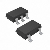
ADR360AUJZ-REEL7 Analog Devices Inc, ADR360AUJZ-REEL7 Datasheet - Page 17

ADR360AUJZ-REEL7
Manufacturer Part Number
ADR360AUJZ-REEL7
Description
IC VREF LP 2.048V 25PPM TSOT23-5
Manufacturer
Analog Devices Inc
Specifications of ADR360AUJZ-REEL7
Temperature Coefficient
25ppm/°C
Reference Type
Series
Voltage - Output
2.048V
Tolerance
±0.29%
Voltage - Input
2.35 ~ 15 V
Number Of Channels
1
Current - Quiescent
190µA
Current - Output
5mA
Operating Temperature
-40°C ~ 125°C
Mounting Type
Surface Mount
Package / Case
TSOT-23-5, TSOT-5, TSOP-5
Topology
Series
Input Voltage
2.45V To 15V
Reference Voltage
2.048V
Reference Voltage Tolerance
6mV
Voltage Reference Case Style
SOT-23
No. Of Pins
5
Operating
RoHS Compliant
Lead Free Status / RoHS Status
Lead free / RoHS Compliant
Current - Cathode
-
Lead Free Status / RoHS Status
Lead free / RoHS Compliant
V
APPLICATIONS
BASIC VOLTAGE REFERENCE CONNECTION
The circuit in Figure 33 illustrates the basic configuration for
the ADR36x family. Decoupling capacitors are not required for
circuit stability. The ADR36x family is capable of driving
capacitive loads from 0 µF to 10 µF. However, a 0.1 µF ceramic
output capacitor is recommended to absorb and deliver the
charge as is required by a dynamic load.
Stacking Reference ICs for Arbitrary Outputs
Some applications may require two reference voltage sources,
which are a combined sum of standard outputs. Figure 34 shows
how this stacked output reference can be implemented.
IN
0.1µF
INPUT
Figure 34. Stacking Voltage References with the ADR36x
0.1µF
0.1µF
Figure 33. Basic Configuration for the ADR36x Family
C1
C2
1
2
3
1
2
3
1
2
3
NC
GND
V
NC
GND
V
NC
GND
V
IN
IN
IN
ADR36x
ADR36x
ADR36x
TRIM
TRIM
V
V
OUT
OUT
5
5
4
4
TRIM
V
OUT
5
4
OUTPUT
0.1µF
V
V
OUT2
OUT1
ADR360/ADR361/ADR363/ADR364/ADR365/ADR366
Rev. 0 | Page 17 of 20
Two reference ICs are used, and fed from an unregulated input,
V
which provides two output voltages, V
the terminal voltage of U1, while V
and the terminal voltage of U2. U1 and U2 are chosen for the
two voltages that supply the required outputs (see Table 10). For
example, if both U1 and U2 are ADR361s, V
V
Table 10. Output
U1/U2
ADR361/ADR365
ADR361/ADR361
ADR365/ADR361
A Negative Precision Reference Without Precision
Resistors
A negative reference is easily generated by adding an op amp,
A1, and is configured in Figure 35. V
ground and, therefore, the negative reference can be taken
directly from the output of the op amp. The op amp must be
dual-supply, low offset, and rail-to-rail if the negative supply
voltage is close to the reference output.
IN
OUT2
. The outputs of the individual ICs are connected in series,
is 5.0 V.
+V
–V
DD
REF
Figure 35. Negative Reference
1
2
3
NC
GND
V
IN
ADR36x
–V
OUT2
DD
OUTF
V
2.5
2.5
5
OUT1
OUT1
is the sum of this voltage
–
+
and V
TRIM
V
and V
OUT
OUT1
OUTS
4
5
OUT2
is 2.5 V and
are at virtual
V
7.5
5.0
7.5
. V
OUT2
OUT1
is


