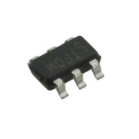
LT6656BCS6-1.25#TRMPBF Linear Technology, LT6656BCS6-1.25#TRMPBF Datasheet - Page 13

LT6656BCS6-1.25#TRMPBF
Manufacturer Part Number
LT6656BCS6-1.25#TRMPBF
Description
IC VREF PREC 5MA 1.25V TSOT23-6
Manufacturer
Linear Technology
Datasheet
1.LT6656BCS6-2.5TRMPBF.pdf
(18 pages)
Specifications of LT6656BCS6-1.25#TRMPBF
Reference Type
Series
Voltage - Output
1.25V
Tolerance
±0.1%
Temperature Coefficient
20ppm/°C
Voltage - Input
2.2 ~ 18 V
Number Of Channels
1
Current - Quiescent
850nA
Current - Output
5mA
Operating Temperature
0°C ~ 70°C
Mounting Type
Surface Mount
Package / Case
TSOT-23-6, TSOT-6
Lead Free Status / RoHS Status
Lead free / RoHS Compliant
Current - Cathode
-
Other names
LT6656BCS6-1.25#TRMPBFTR
Available stocks
Company
Part Number
Manufacturer
Quantity
Price
Typical applicaTions
Regulator Reference
The robust input and output of the LT6656 along with its
high output current make it an excellent precision low
power regulator as well as a reference. The LT6656 would
be a good match with a small, low power microcontroller.
Using the LT6656 as a regulator reduces power consump-
tion, decreases solution size and increases the accuracy
of the microcontroller’s on board ADC.
3V ≤ V
IN
≤ 18V
Figure 12. Microcontroller Reference and Regulator
0.1µF
IN
LT6656-2.5
OUT
10µF
5.1V ≤ V
IN
≤ 18V
MCU
PB1/INT0/A
0.1µF
PB2/ADC1/SCK/T0/INT0
PB0/AIN0/A
V
PB5/RESET/ADC0
Figure 13. Low Power ADC Reference
CC
GND
IN1
/V
/MISO/OC1A
REF
IN
PB3/ADC2
PB4/ADC3
REF
/MOSI
6656 TA02
LT6656-5
DIFFERENTIAL INPUT
AT 1sps, I
5
6
7
2
3
1
±V
REF
OUT
• 0.5 (±2.5V)
Q
= 27.4µA
Low Power ADC Reference
Low power ADCs draw only a few µAs during their idle
period and well over 100µA during conversions. Despite
these surges of current, the ADC in reality can have very
low power consumption. Figure 13 shows the LTC2480, a
low power delta sigma ADC. When the ADC is disabled its
quiescent current (I
I
is not only based on the I
power consumption of the ADC is set by the conversion
time and the sample rate. The LTC2480 shown in Figure 13
has a conversion time of 160ms which sets the maximum
sample rate of 6 samples per second. The maximum sample
rate also sets the maximum current consumption to 160µA,
but at slower sample rates the ADC will have significantly
lower average current draw. If the ADC is sampled at 1
sample per second the average current drawn by the ADC
during a 1 second interval would only be 26.4µA. When
taking into consideration the current drawn by the refer-
ence, the total current draw is only 27.4µA. This system is
greatly simplified because the precision reference does not
need to be cycled on and off to save power. Furthermore,
leaving the reference on continuously eliminates concern
for turn-on settling time.
Q
jumps up to 160µA. In reality, the power consumption
4.7µF
IN
IN
+
–
REF
LTC2480
Q
V
) is roughly 1µA, during conversion the
CC
SDO
SCK
CS
Q
6656 TA05
during conversion, but the real
LT6656
6656fa


