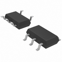
LT6650HS5#TRM Linear Technology, LT6650HS5#TRM Datasheet - Page 7

LT6650HS5#TRM
Manufacturer Part Number
LT6650HS5#TRM
Description
IC REF 400MV R-R BUFFER TSOT23-5
Manufacturer
Linear Technology
Datasheet
1.LT6650CS5TR.pdf
(12 pages)
Specifications of LT6650HS5#TRM
Reference Type
Series
Voltage - Output
400mV
Tolerance
±1.5%
Temperature Coefficient
30ppm/°C
Voltage - Input
1.4 ~ 18 V
Number Of Channels
1
Current - Quiescent
11µA
Current - Output
200µA
Operating Temperature
-40°C ~ 125°C
Mounting Type
Surface Mount
Package / Case
TSOT-23-5, TSOT-5, TSOP-5
Lead Free Status / RoHS Status
Contains lead / RoHS non-compliant
Current - Cathode
-
Other names
LT6650HS5
LT6650HS5
LT6650HS5
Available stocks
Company
Part Number
Manufacturer
Quantity
Price
PI FU CTIO S
BLOCK DIAGRA
APPLICATIO S I FOR ATIO
FB (Pin 1): Resistor Divider Feedback Pin. Connect a
resistor divider from OUT to GND and the center tap to FB.
This pin sets the output potential.
GND (Pin 2): Ground Connection.
DNC (Pin 3): Do not connect. Connected internally for post
package trim. This pin must be left unconnected.
Long Battery Life
The LT6650 is a micropower, adjustable reference which
operates from supply voltages ranging from 1.4V to 18V.
The series regulated output may be configured with exter-
nal resistors to any voltage from 400mV to nearly the
supply potential. Under no-load conditions, the LT6650
dissipates only 8µW when operating on a 1.4V supply.
Other operating configurations allow the LT6650 to be
used as a micropower positive or negative adjustable
shunt reference from 1.4V to 18V.
Bypass and Load Capacitor
The LT6650 voltage reference requires a 1µF or greater
output capacitance for proper operation. This capacitance
may be provided by either a single capacitor connected
between OUT and GND or formed by the aggregate of
several capacitors that may be serving other decoupling
U
U
U
U
U
W
W
DNC
3
U
V
REFERENCE
R
= 400mV
GND
IN
4
2
+
–
IN (Pin 4): Positive Supply. Bypassing with a 1µF capacitor
is recommended if the output loading changes.
OUT (Pin 5): Reference Output. The output sources and
sinks current. It is stable with any load capacitor with a
total capacitance of 1µF or more. Higher load capacitance
improves load transient response.
functions. Output impedance can be reduced by DC load-
ing of the output by 40µA to 200µA, and/or adding an R
to the output capacitor for a 100µs time constant as shown
in Figure 1 and the Typical Performance Characteristics
graphs.
The LT6650 Voltage reference should have an input by-
pass capacitor of 0.1µF or larger. When the circuit is
V
IN
R
IN
LT6650
Figure 1. LT6650 Input-Output Configuration
6650 BD
C
IN
5
1
IN
OUT
FB
4
LT6650
2
GND
6650 F01
5
1
OUT
FB
LT6650
R
Z
C
6650fa
L
7
V
OUT
Z


