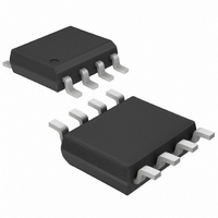
MAX6190AESA Maxim Integrated Products, MAX6190AESA Datasheet - Page 2

MAX6190AESA
Manufacturer Part Number
MAX6190AESA
Description
IC VOLT/REF MICRO PWR LDO 8-SOIC
Manufacturer
Maxim Integrated Products
Datasheet
1.MAX6190CESA.pdf
(14 pages)
Specifications of MAX6190AESA
Reference Type
Series
Voltage - Output
1.25V
Tolerance
±2mV
Temperature Coefficient
5ppm/°C
Voltage - Input
2.5 ~ 12.6 V
Number Of Channels
1
Current - Quiescent
35µA
Current - Output
500µA
Operating Temperature
-40°C ~ 85°C
Mounting Type
Surface Mount
Package / Case
8-SOIC (3.9mm Width)
Product
Voltage References
Topology
Series References
Output Voltage
1.25 V
Average Temperature Coefficient (typ)
2 PPM / C
Series Vref - Input Voltage (max)
13.5 V
Shunt Current (max)
0.5 mA
Maximum Operating Temperature
+ 85 C
Minimum Operating Temperature
- 40 C
Mounting Style
SMD/SMT
Lead Free Status / RoHS Status
Contains lead / RoHS non-compliant
Current - Cathode
-
Available stocks
Company
Part Number
Manufacturer
Quantity
Price
Part Number:
MAX6190AESA
Manufacturer:
MAXIM/美信
Quantity:
20 000
Company:
Part Number:
MAX6190AESA+T
Manufacturer:
MAXIM
Quantity:
393
Company:
Part Number:
MAX6190AESA-T
Manufacturer:
MAXIM
Quantity:
1 516
Company:
Part Number:
MAX6190AESA-T
Manufacturer:
MAXIM
Quantity:
2 126
Part Number:
MAX6190AESA.
Manufacturer:
MAXIM/美信
Quantity:
20 000
ABSOLUTE MAXIMUM RATINGS
Voltages Referenced to GND
Output Short Circuit to GND or IN (V
Output Short Circuit to GND or IN (V
Continuous Power Dissipation (T
Precision, Micropower,
Low-Dropout Voltage References
ELECTRICAL CHARACTERISTICS—MAX6190
(V
2
Stresses beyond those listed under “Absolute Maximum Ratings” may cause permanent damage to the device. These are stress ratings only, and functional
operation of the device at these or any other conditions beyond those indicated in the operational sections of the specifications is not implied. Exposure to
absolute maximum rating conditions for extended periods may affect device reliability.
OUTPUT
OUTPUT
Output Voltage
DYNAMIC
INPUT
Output-Voltage Temperature
Coefficient (Note 1)
Line Regulation
Load Regulation
Short-Circuit Current
Temperature Hysteresis
(Note 2)
Long-Term Stability
DYNAMIC
Noise Voltage
Ripple Rejection
Turn-On Settling Time
Capacitive-Load Stability Range
INPUT
Supply Voltage Range
Quiescent Supply Current
Change in Supply Current
IN ......................................................................-0.3V to +13.5V
OUT ..........................................................-0.3V to (V
IN
8-Pin SO (derate 5.88mW/°C above +70°C)................471mW
_______________________________________________________________________________________
= 5V, I
PARAMETER
OUT
= 0nA, T
A
= T
MIN
A
to T
= +70°C)
SYMBOL
V
IN
IN
TCV
∆V
∆V
∆V
∆V
OUT
I
∆I
C
V
cycle
e
IN
MAX
∆V
time
< 6V) ............Continuous
≥ 6V) .........................60s
I
V
OUT
OUT
I
OUT
OUT
SC
t
OUT
OUT
OUT
OUT
IN
/V
R
IN
OUT
IN
/V
IN
, unless otherwise noted. Typical values are at T
IN
/
/
/
/
T
MAX6190A
MAX6190B
MAX6190C
2.5V ≤ V
Sourcing: 0 ≤ I
Sinking: -500µA ≤ I
Short to GND
Short to IN
1000hrs at +25°C
0.1Hz to 10Hz
10Hz to 10kHz
V
To 0.1%, C
(Note 3)
Guaranteed by line-regulation test
2.5V ≤ V
A
IN
= +25°C
= 5V ±100mV, f = 120Hz
IN
IN
IN
+ 0.3V)
≤ 12.6V
≤ 12.6V
OUT
OUT
= 50pF
CONDITIONS
OUT
≤ 500µA
Operating Temperature Range ...........................-40°C to +85°C
Junction Temperature ......................................................+150°C
Storage Temperature Range .............................-65°C to +150°C
Lead Temperature (soldering, 10s) .................................+300°C
Soldering Temperature (reflow) .......................................+260°C
≤ 0
MAX6190A
MAX6190B
MAX6190C
A
= +25°C.)
1.248
1.246
1.244
MIN
2.5
0
1.250
1.250
1.250
TYP
0.12
0.15
0.8
75
50
25
65
86
30
27
2
4
8
8
4
4
1.252
1.254
1.256
MAX
12.6
0.5
0.6
2.2
10
25
80
35
5
2
1000hrs
ppm/°C
UNITS
µV
µV/µA
µV
ppm/
µV/V
ppm
µA/V
mA
dB
µA
nF
µs
RMS
V
V
P-P


